In recent decades, electronic technology has developed rapidly and has become more and more widely used. It has become an important part of modern science and technology. What is electronic technology? Simply put, electronic technology is the science and technology to study electronic devices, electronic circuits and their applications. Learning analog electronics will lay the foundation for us to further study the content in the field of electronic technology and the application of electronic technology in the profession.
Starting with the formation of a pN junction, the semiconductor diode and its application are known.
1. Intrinsic semiconductor: pure crystal structure covalent bond free electron hole (pair in appearance) ie carrier (2 species) [hole current electron current]
Features: high resistivity, electrical conductivity with temperature changes
2, doped semiconductor
a: N-type semiconductor: doped with a pentavalent element impurity (donor impurity), and the free electron is a multi-sub (the majority carrier is called a multi-sub).

Hole is the minority
The concentration of the multiplier is related to the concentration of the impurity incorporated rather than the temperature, and the concentration of the minority is related to the temperature.
b: P-type semiconductor: doped with trivalent element (boron) acceptor impurity, hole is multi-sub, free electron is minority
If the impurity concentration of the pentavalent element is more than the concentration of the trivalent impurity, the P type can be turned to the N type.
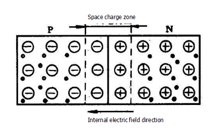
3. Formation of PN junction
Multi-sub-concentration on both sides - multi-sub-diffusion - forming an internal electric field - hindering multi-sub-motion - enhancing the drift of the few children - drifting and spreading to achieve dynamic equilibrium - forming a PN junction
Note: Due to the large difference in multi-sub-concentration between the N-type semiconductor and the P-type semiconductor on both sides of the interface, the multi-substrate on the P-type semiconductor side is a hole, and its concentration is much larger than that of the N-type semiconductor; N-type semiconductor The multiple molecules on the side are electrons, and their concentration is much larger than that of the P-type semiconductor side. This concentration difference causes the multiple sub-diffusions to reach each other through the interface, and recombines with the other's multiple sub-subjects, so that the P-region forms a thin film layer with no holes and only negative ions near the interface; the N region forms a lack near the interface electron, only a thin layer of positive ions.
4. Unidirectional conductivity of PN junction
a: forward bias of the PN junction P—the positive pole of the power supply N—the negative pole of the power supply. The external electric field weakens the internal electric field, the dynamic balance breaks, the multi-sub-diffusion motion is strengthened, and the minority carrier drift motion is weakened, forming a forward current—the PN guide through
b: reverse bias of the PN junction P - negative power supply N - positive power supply, then PN cutoff
5. Relationship between current and voltage on pN junction
There is a relationship such as IF=Isexp(-eVF/kT), where -e is the electron charge; k is the Boltzmann constant; T is the absolute temperature; Is is the reverse saturation current, and the forward voltage U>0, i=Isexp(U/ut); Reverse voltage U<0, i=IS (I is independent of U).
If you want to know more, our website has product specifications for the semiconductor diode, you can go to ALLICDATA ELECTRONICS LIMITED to get more information


没有评论:
发表评论