2019年7月30日星期二

What are the methods of shielding interference in PCB design?

The transmission rate of high-speed PCB design and wiring systems is steadily increasing, and it also brings some kind of anti-interference vulnerability. The higher the frequency of transmitting information, the increased sensitivity of signals, and their energy is getting weaker. The wiring system at this time is more susceptible to interference. Interference is ubiquitous, andcables and equipment can interfere with other components or be severely interfered with by other sources of interference, such as computer screens, mobile phones, electric motors, radio equipment, data transmission, and power cables. In addition, potential eavesdroppers, cybercrime and hackers are increasing because they can cause huge damage and loss in the interception of UTP cable information.

Especially when using high-speed data networks, the time required to intercept large amounts of information is significantly lower than the time required to intercept low-speed data transmissions. The twisted pair in the data twisted pair can resist its external interference and crosstalk between the pairs at its low frequency, but at high frequencies (especially when the frequency exceeds 250MHz), Wire twisting has not been able to achieve the purpose of anti-interference, only shielding can resist external interference.

The cable shield acts like a Faraday shield, and the interfering signal enters the shield but does not enter the conductor. Therefore, data transmission can run without problems. Since shielded cables have lower radiated emissions than unshielded cables, network transmissions are prevented from being intercepted. Shielded networks (shielded cables and components) can significantly reduce the level of electromagnetic radiation that can be intercepted into the surrounding environment.
The shielding field of different interference fields is mainly composed of electromagnetic interference and radio frequency interference. Electromagnetic interference (EMI) is mainly low frequency interference, and motors, fluorescent lamps, and power lines are common sources of electromagnetic interference. Radio Frequency Interference (RFI) refers to radio frequency interference, mainly high frequency interference. Radio, television, radar and other wireless communications are common sources of RF interference. For resisting electromagnetic interference, the choice of braided shield is most effective because it has a lower critical resistance; for radio frequency interference, the foil layer shielding is most effective, because the braided shield depends on the wavelength change, and the gap created by it makes the high frequency signal free. In and out of the conductor; for high-low frequency mixed interference field, a combination of foil layer and woven mesh with broadband coverage is used. In general, the higher the mesh shielding coverage, the better the shielding effect.
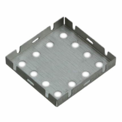
image.png 

2019年7月29日星期一

How to set parameters of the inverter?

Inverter parameter setting (1)
There are many setting parameters of the inverter, each parameter has a certain range of selection. In use, it is often encountered that the inverter cannot work normally due to improper setting of individual parameters. Therefore, the relevant parameters must be correctly set.

1. Control mode: speed control, torque control, PID control or other methods. After the control method is adopted, static or dynamic identification is generally performed according to the control precision.

2, the lowest operating frequency: that is, the minimum speed of the motor running, when the motor runs at low speed, its heat dissipation performance is very poor, the motor running at low speed for a long time, will cause the motor to burn. At low speeds, the current in the cable also increases, which can also cause the cable to heat up.

3, the highest operating frequency: the general frequency of the inverter to 60Hz, and some even to 400 Hz, high frequency will make the motor run at high speed, this for ordinary motors, its bearings can not run for a long time at the super rated speed, the motor Whether the rotor can withstand such centrifugal force.

4, carrier frequency: the higher the carrier frequency setting, the higher the harmonic component, which is closely related to the cable length, motor heating, cable heating inverter heating and other factors.

5. Motor parameters: The inverter sets the power, current, voltage, speed and maximum frequency of the motor in the parameters. These parameters can be directly obtained from the motor nameplate.

6. Frequency hopping: At a certain frequency point, resonance may occur, especially when the whole device is relatively high; when controlling the compressor, the surge point of the compressor should be avoided.

Inverter parameter setting (2)
There are many function parameters of the inverter, generally there are dozens or even hundreds of parameters for the user to choose. In practical applications, it is not necessary to set and debug each parameter, and most of them only need to adopt the factory setting value.

First, acceleration and deceleration time
The acceleration time is the time required for the output frequency to rise from 0 to the maximum frequency, and the deceleration time is the time required to fall from the maximum frequency to 0. The acceleration and deceleration time is usually determined by the frequency setting signal rising and falling. When the motor is accelerating, the rate of increase of the frequency setting must be limited to prevent overcurrent, and when decelerating, the rate of decrease is limited to prevent overvoltage.

Acceleration time setting requirement: Limit the acceleration current below the overcurrent capacity of the inverter, and do not cause the inverter to trip due to the over-speed. The deceleration time setting point is: prevent the smoothing circuit voltage from being too large, and the regenerative overvoltage stall is not caused. Let the frequency converter trip. The acceleration/deceleration time can be calculated according to the load. However, in the commissioning, the long acceleration/deceleration time is set according to the load and experience. The motor is observed by the start and stop motors to see if there is overcurrent or overvoltage alarm. Then the acceleration/deceleration setting time is gradually Shorten, the principle of no alarm occurs during operation, and repeat the operation several times to determine the optimal acceleration and deceleration time.

Second, the torque boost
Also called torque compensation, it is a method to increase the low frequency range f/V to compensate for the torque reduction at low speed caused by the stator winding resistance of the motor. When set to automatic, the voltage during acceleration can be automatically increased to compensate for the starting torque, so that the motor accelerates smoothly. If manual compensation is used, a better curve can be selected by experiment depending on the load characteristics, especially the starting characteristics of the load. For variable torque loads, if the selection is improper, the output voltage will be too high at low speed, and the phenomenon of wasting electric energy may even occur when the motor is loaded with load and the current is not high.

This article is from Allicdata Electronics Limited which offers electronic components, semiconductors, antennas, capacitors, connectors, diodes, transistors, ICs, resistors

For more product information, please go to the website to get it.


What is the role of voltage transformer in the ATX power?

The voltage transformer plays a role from front to back in the ATX power supply. The electrical energy input from the primary winding is converted into magnetic energy stored in the core. The magnetic field stored in the transformer core requires a secondary winding output to the rear stage at a "suitable" time via a voltage-varying secondary winding. So, what's the right time? Let's analyze this problem through real-life examples.

1.Cases of  reservoir storage for power generation.
 After a certain amount of water is stored in the reservoir, it can start to generate electricity. At the same time, upstream incoming water can continue to flow into the reservoir and accumulate. This means that there are inputs (upstream water) at the same time as output (power generation) for reservoirs linking up and down.

2.Cases of charging and discharging of rechargeable battery

 After the rechargeable battery has run out of power, it needs to be recharged. Only after recharging, can it be installed into the device to provide the equipment with normal electrical energy.
This means that there is no output (discharge) for a rechargeable battery with input (charge) at the same time.
But why many battery-powered devices (such as laptops) can be charged at the same time?This is actually an illusion, because it is the AC 220V, not the rechargeable battery, that supplies the device with normal power at the moment.

So, is the switching transformer, like reservoir storage, able to output electricity through secondary windings at the same time as charging, or is it possible to output electrical energy through secondary windings after charging and discharging of rechargeable batteries? The answer is: yes, just avoid oversaturation of the core of the switching transformer It is referred to as "forward" (analogy to reservoir energy reserve) in the process of transformer energy conversion which outputs electrical energy through secondary windings at the same time as the primary winding is charged with energy. This is referred to as "fly back" (analogy to charging and discharging of a rechargeable battery) for a transformer that converts energy after the primary winding is charged and then outputs electricity through the secondary winding.

Visible, "forward" and "fly back" are not in fact based on the direction of energy transfer (the direction of any switching power supply is fixed, from the primary winding to the secondary winding), It's a distinction based on the transmission time of energy. Therefore, forward and fly back are essentially the concepts of time related to energy storage, transfer (release).
For "single-transistor forward" and "double-transistor forward" ATX power supplies, the primary switching transformer, while charging the primary windings, has begun to output electricity to subsequent rectified circuits through secondary windings. This is the meaning of "forward" in "single-tube forward" and "double-tube forward".

"fly back" is suitable for low power applications, while "forward" is more suitable for higher power applications. In the ATX power supply, the auxiliary power supply is small, basically uses the "fly back", and the main power supply is large, basically uses "forward". Although there is no word "forward" in the "two-tube and half-bridge" topology, it is actually a form of "forward".

This article is from Allicdata Electronics Limited. Reprinted need to indicate the source.

Different roles of different resistors in the circuit

1.Protective resistor.
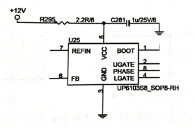
The function of the protective resistor is to protect the main components of the circuit from burning out. In figure 1, R295 is used to protect the resistor. When the chip U25 is overloaded or short-circuited, the current through the resistor R295 becomes larger. When the resistance is beyond the range that the resistor can withstand, the resistance spontaneous combustion causes the circuit to be open and the chip power supply is disconnected. Thus protecting the front 12 V main power supply circuit from being damaged. The protective resistor is generally below 10 Ω.    
                   image.png
                Fig.1 Protective resistor application circuit


2. Pull up resistor.
The role of the pull up resistor is to pull the uncertain signal to a high level to increase the signal current, so that the signal can be transmitted at long distance and at high speed. In figure 2, the RN3 is a pull-up resistor. The LDT_RST# signal is pulled up through the RN3 to the VCC_DDR voltage to increase the working current, and the pull-up resistor also acts as a finite current.

3. Pull down resistor.
The pull-down resistor is used to set the working state of the signal by grounding the uncertain signal through the resistor. Figure 3 the PGNT#0 signal is grounded through the pull-down resistor R608, setting the PGNT#0 signal to a low level state. The pull-down resistor on the signal line absorbs the current, absorbs the current of the output signal to the GND, and reduces the impact of the signal on the back stage circuit.
                        image.png
       
                                 Fig.2 Pull up resistor              Fig.3 Pull-down resistor      
                               application circuit                             application circuit

4. Partial voltage resistor.
The circuit with both pull up resistor and pull-down resistor is called divider circuit. A suitable voltage can be obtained by a normal power supply. Divider resistors are used in power supply circuits or reference voltage circuits with low current. The R424 and R423 in figure 4 form a voltage divider circuit. The R424 connection power supply is called the upper resistor, the R423 grounding is called the lower resistance. After the 1_5VREF voltage is divided by R424 and R423, the DDR3_1_5REF voltage is obtained as the reference voltage to the memory.

5. The resistance is judged.
The method of measuring the resistor is shown in figure 5. The digital multimeter is adjusted to the ohmic block, the two multimeter pens contact the two ends of the resistor, and the value of the measured resistance is displayed on the display screen. If the measured value does not match the resistor indicator, the measured resistor is damaged.
 1552619495801124.png
     
 Fig.4 Resistive partial voltage application circuit                 Fig.5 Resistance measurement

Note that:
(I) resistor damage is generally shown as a larger resistance or open circuit.    
(2) because of the different materials of the resistor, the resistance value will have certain error, the resistance within the error range of the measurement value belongs to the good resistor.
(3) when accurate measurement is needed, the resistor must be removed and measured.

Allicdata Electronic specialize in the production of resistors includes chassis mount resistors,through hole resistors,resistor networks,arrays,etc. If you are sourcing the products, please contact us, we will try our best to solve it for you. For more product information, please go to the website to get it.

2019年7月26日星期五

What are the advantage of FPGAs than ASICs?

 Traditional design methods using only ASSP or ASIC have major drawbacks. The functionality of ASSP is prefabricated and it is difficult to support the latest technology, which manufacturers cannot use to highlight product advantages. The ASIC has a long development cycle and is difficult to adapt to the short product cycle of the consumer market. Therefore, the new design approach should be very flexible, can be quickly innovated, and start-up development costs are low. For system designers, this means using a combination of programmable logic devices (PLDs) and ASICs or ASSPs to remain competitive in the consumer electronics market, respond flexibly to changes in demand, and highlight product advantages.
ASSP: Special Standard Products
ASIC: ASIC

Relying solely on ASICs and ASSPs will force manufacturers to postpone product releases, resulting in outdated product functionality. The PLD/ASIC-ASSP approach ensures rapid innovation and a leading position in the industry. When designing increased throughput, this design approach can effectively combine FPGA-to-structured ASIC migration to achieve rapid, low-risk mass production.

FPGA advantages:
Low power consumption
Flexible and programmable
The consumer electronics market is very demanding on the cost and power requirements of the product. In addition, product differentiation is also the key to manufacturers' success. The programmable nature of the FPGA gives the product the unique flexibility to implement any digital circuit you want to implement, and you can customize a variety of circuits. The advantages of FPGA in the field of consumer electronics are reflected in a "fast" word with a short development cycle.

FPGA flexibility is reflected in the reduction of the constraints of dedicated chips, truly tailored to their own products, FPGAs can be flexibly changed design during the design process. And its powerful logic resources and register resources allow you to easily use the design concept, its parallel execution, hardware implementation can deal with a large number of high-speed electronic circuit design needs in the design.
Another benefit of using FPGA's programmable features is that it can reduce inventory. System vendors use the same PCB to support different market needs and functions around the world, and each configuration can achieve different functions.
On the whole, FPGAs have shorter design cycles and flexibility than ASICs (dedicated chips), which are ideal for products that need to be quickly brought to market, eliminating the need for expensive opening costs, and can be cut at any time to increase the functionality you want. Achieve evasion of design risks and avoid the limitations of chip manufacturers. In addition, with the advancement of technology, the NRE (one-time engineering) cost required for ASIC products is getting higher and higher. Due to the constraints of enterprise R&D funds, ASIC has been replaced by FPGA in many market segments.

2019年7月24日星期三

What is the structure of the moving coil microphone and how is it detected?

Moving coil microphone. Generally known as a microphone.


It is an acoustic and electrical converter. A moving coil microphone consists of a diaphragm, a coil, a permanent magnet, and an output transformer. The diaphragm vibrates with sound pressure and drives the coils in it to vibrate in the magnetic field to generate an induced current. The current changes with the sound pressure of the diaphragm. The greater the sound pressure, the greater the current generated. The lower the sound pressure, the smaller the current generated (usually a few mV). An output transformer is also attached to the microphone to improve sensitivity and to match the amplifier's impedance. Transformers have two types of self-coupling and mutual inductance. There are two types of output impedance, high resistance and low resistance, depending on the turns ratio of both side coils. The output impedance of the microphone is less than 600 ohms, and it is a low resistance microphone. The output impedance is higher than 10,000 ohms and is a high resistance microphone.


Detect moving coil microphone


 (1) To detect the appearance of the structure, adopt the method of the first outside and back, if there is distortion, the sense of steel is broken, first whether the lower sound head is affected A table to check if the value of each round is similar or not.


If a silent failure occurs, first make sure that the next voice coil wiring is loose and loose, and then use a multimeter to check if it is on or off. You also need to make sure that the switch is loose, the plug is welded, and that the cord and shield are open.

https://www.allicdata.com/list.html?category_id=1925


(2) Judgment of silent


Common microphones (such as family karaoke microphones), their DC resistance is 600Ω. Test the center end of the plug with a multimeter RX100Ω and open the microphone switch ON. The resistance is 600Ω. If the impedance is not measured, it is explained that there is a break in the plug switch head. This can be detected with a multimeter.


First, unscrew the front cover and measure both ends of the lead extraction line directly. Using R will prove that the inside of the voice coil is open. If R is about 600 ohms, the voice coil is good and the fault is in the plug or wire rope and switch. In such places, it is actually proven that the phenomenon of disconnection occurs frequently. For example, the screen cable capacity of the wire rope is fragile, the core wire is welded, the switch's internal contact is bad, or the connection is bad, solder removal.


(3) Serious calls are a common drawback of microphones, which are mainly caused by the following reasons. The shield cable in the cord is broken or the shield wire connected to the plug is disconnected, and only the core wire is normal. When the plug of the microphone is inserted into the socket of the amplifier, the shield wire is cut, so the ground wire is also cut, and the human body's induction and the external interference of the hand microphone are transmitted to the self-oscillation of the loudspeaker. . After replacing the sound head, the core and screen are lined with thin lines, so the two wiring terminals of Ye to the sound head will pass, so it is easy to activate the centerline docking power amplifier. The device's ground terminal screen is connected to the power amplifier's input terminal.


The microphone of the plastic cylinder shell is not a problem and does not cause howling, but the centerline is connected to a metal case, and the induction of the human body causes a power amplifier to generate howling. Use the multimeter RX100 Ω to block the test. One end of the sound head is welded so as not to form a circuit. Then turn the switch to the "ON" position. Placing it in the "OFF" position will also affect the circuit as well as shortening the center and shield lines, which will affect the test. Then use a multimeter to connect the center end of the plug to the metal shell of the microphone. The practical model prevents the human body from sensing that the core wire is not connected to the handheld metal part. Since the metal cylinder shell is connected to the terminal of the plug shield wire, there is no howling because the earth portion of the power amplifier is fixed.

https://www.allicdata.com


 (4) In order to detect the light and distortion of the acoustic head, loosen the front cover of the acoustic head and observe whether the vibrating film is compressed and has no elasticity. Use two stylus points at the ends of the touchhead, a multimeter RX1 file. If the sound is very low, use RX100 Ω to measure the impedance. If the impedance is about 300 ohms, a short between turns exists in the voice coil, which is

Method of measuring IGBT

(1) Measure 3 feet of IGBT with multimeter RX10kΩ without damping tube. One of them is infinity at the other two feet, this foot is at G, the other two feet are at C and E.

In the test, there are two legs with specific resistance, small resistance such as NPN type pipe, black pen is connected to E, red pen is connected to C. PNP type is the opposite.


(2) Three-electrode measurement with RX10Ω to RX100Ω for attenuation tube measurement. The secondary resistance is hundreds of ohms, the other is thousands of ohms. The two legs are C and E, the resistance is small, the black pen is the E pole, the red stylus is the C pole, and the other foot is the B pole (G pole).


(3) When measuring IGBT modules, it is necessary to measure the resistance between IGBT's CE, CB, and BE using a multimeter RX10Ω matched to the resistance of the attenuation meter. If an IGBT component fails, there may be a short between the collector and the emitter, and the collector and the gate. (Note: When the IGBT operates, the voltage between the gate and the emitter is about 9 V and the emitter is the reference. When using the road measurement method, first cut the corresponding pins to prevent the circuit due to the influence of the circuit You need to make an internal resistance by mistake.


If you want to know more, our website has IGBT product specifications, you can go to Allicdata Electronics Limited to get more information.


IGBT: HGTD1N120BNS9A
HGTD1N120BNS9A Allicdata Electronics
IGBT module : IXGN320N60A3
IXGN320N60A3 Allicdata Electronics

2019年7月23日星期二

What is the procedure for capacitor step-down?

Capacitor step-down LED driver circuits are often used in small current LED drive circuits because of their small size, low cost, and relative constant current.


The capacitor buck LED driver circuit uses the capacitive reactance generated by the capacitor with a specific AC number to limit the maximum operating current. For example, at an operating frequency of 50%, a capacitive reactance of approximately 3180Ω occurs with a 1μF capacitor. When an AC voltage of 220 volts is applied to the capacitor, the maximum current flowing through the capacitor is about 70 yen cheaper. However, if the capacitor is an ideal capacitor, the current flowing through the capacitor is an imaginary current, and the work is a low power, so no power is generated in the capacitor (the capacitor belongs to the energy storage component).


According to this feature, when the resistive element is connected in series on the 1 μF capacitor, the voltage obtained across the resistive element and the power dissipation that it generates are completely dependent on the characteristics of the resistive element.

For example, connect a 110V / 8W bulb in series with a 1uF capacitor and connect it to an AC voltage of 220V / 50Hz. The bulb lights up and becomes normal brightness without burning because the 110V / 8W bulb needs 8W / 110V = 72mA. This is consistent with the current limiting characteristics of the 1uF capacitor.

Similarly, if you connect a 65V / 5W cell and a 1uF capacitor in series to a 220V / 50Hz AC, the cell will light without burning, since the operating current of the 65V / 5W cell is also about 70mA. Thus, the capacitor bucking actually uses capacitive reactance current limiting, and the capacitor acts as a limiting current, dynamically distributing the voltage across the capacitor and load.


The traditional way of converting AC power to low voltage DC is to rectify and filter after bucking using a transformer. When limited by factors such as capacity and cost, the easiest and most practical method is to use a capacitor buck power supply.


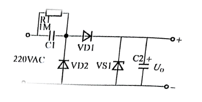
When switching the circuit, it is necessary to first determine the correct value of the load current and then select the capacity of the step-down capacitor. Capacitor step-down application circuit diagram as shown in the figure below
image.png
In fact, the charge and discharge current flowing through C1 increases as the charge / discharge current ICC1 flowing through C1 increases and the capacitive reactance XC decreases as the charge / discharge current ICC1 flowing through C1 increases. . If the current Xin Yi is smaller than the charge / discharge current of C1, the maximum capacity current of the zener diode where the excess current flows in the zener Idmax is Ic-like. If it is smaller than X1, then it is necessary to make the selection of the withstand voltage more than twice the power supply voltage in order to operate C1 which makes the zener diode easy to burn. The bleeder resistor R1 needs to be selected to release the C1 charge for the required time.


This article is from Allicdata Electronics Limited.

IO chip and clock chip on computer motherboard

1. IO chip

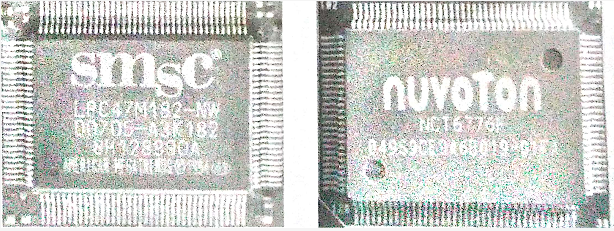
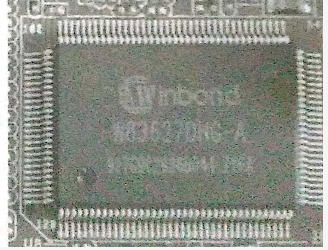
IO stands for I / O Manager. Some Q / S2 interface, serial port, parallel port, front panel, fan, etc. Combined with IO chip control. Common IO chip brands for mainboard maintenance are Fukoku, Itokin Fintek, SMSC, and Tangen (see Figure 1).
image.png
(A) Winbond IO chip (b) iTE IO chip (c) Fintek IO chip
image.png
(D) SMSC IO chip (e) nuvoTon IO chip

Figure 1 IO chip
https://www.allicdata.com/products.html
When replacing 10 chips in mainboard maintenance, it is important to pay attention to whether they are special to the manufacturer of the motherboard. For example, 华 Co., Ltd. The 10 chips for the final model A are dedicated to the kite (see Figure 2).
image.png

What is a Digital / Analog Multimeter?

There are two common digital / analog multimeters.

1. Digital / analog hybrid multimeter.

This type of multimeter adds 7/2 digits to the analog multimeter.


Digital / Analog Bar Chart Double Display Digital Multimeter.

The children of this multimeter are used to observe the analog amount of continuous variation (such as the change in UC during capacitor charging and discharging). Typical products include DT96OT (7/2 digit / 41 bar), 2 BY1935 (15/4 digit / 31 segment) and EDM83B (19/4 digit / 43 segment).

The simulated bar chart has two meanings.


(1) It is determined as a continuous variation analog.


(2) The measured variation is simulated in the form of a bar graph. Bar charts, also called bar charts, can play the role of pointers. The simulated bar graphs are divided into the following three categories:

1 liquid crystal (LCD) bar graph.

The liquid crystal (LCD) bar graph is an intermittent bar, which has high resolution, low power consumption, and low voltage drive, which is suitable for battery-powered miniaturized equipment. The disadvantage is that it is not easy to observe at night.

https://www.allicdata.com/list.html?category_id=2086

Amber Plasma (PDP) Optical Column Display

The advantages of plasma (PDP) optical column display are self-emission, high brightness, bright display and long viewing distance, but the disadvantages are high driving voltage and large power dissipation.


LED The LED array consists of high-intensity, low-cost multiple light-emitting diodes, but the consumption of power is limited.


This article is from Allicdata Electronics.

New amplifiers with audio applications-ICs and multichip modules

Infineon has proposed four new Merus brand IC amplifiers that combine existing amplifier products with audio applications (ICs and multi-chip modules).


With the new “Merus” brand for audio amplifier ICs, Infineon wants to surpass the advantages of amplifier ICs.

1. When sound is generated by the speaker, で is not distributed.

I can not cry but I can see it.

Small and light.

4. Flexible and determinable, but not only difficult to use with textiles.


The Merus amplifier is based on a new technology: multi-stage switching technology for audio and video amplifiers, multi-level converter technology It not only provides high efficiency, but also sound quality, size, output power, electromagnetic radiation and It also has a good influence on other audio amplifiers like parts cost.


Under the new Merus brand, Infineon bundles amplifier ICs for audio applications.

Infineon is transforming a new d 级 audio amplifier to control the power level of an analog 5-speed converter. These multistage d 级 amplifiers use additional power MOSFETs (built into the IC) and capacitors compared to conventional amplifiers.

This technique makes it possible to output audio signals with higher granularity, ie higher switching frequency and scalable output signal levels. Another advantage of the multistage d 级 amplifier is that it allows for a small 设计 and sleep mode with little measurable switching losses.


Four new Merus amps

Based on the new transformation technology, Infineon incorporates one of four integrated multi-stage d 级 audio amplifiers: MA12040 and MA12070 with analog audio input, MA12040P and MA12070P with digital input (I 2 S). Satisfied with the power consumption of the 250 毫 tile range, there is no output filter. Therefore, it is particularly suitable for portable battery drive devices and applications where the installation space is limited (when there is no space for a heat sink and there is an output filter).


The new Merus Class D amps of the UK MA12040 / P and MA12070 / P support up to 4 channels.

Conventional d 级 amplifiers operate only at higher volume levels and are more efficient. A realistic and typical audio playback that requires an average of about 1 watt of output power on its own is much higher power than the IC of the first generation Merus multi-stage class d audio amplifier currently presented .

The new audio amplifier IC supports up to 4 channel modes: PBTL (parallel bridge load), BTL (bridge load), or SE (single end) can be set. In PBTL mode, 16 large load currents in a single monolithic IC. Alternatively, a 4-channel IC can be used in the 2.1 system. For example, two drive a 20 watt range speaker (SE mode) and a 40 W woofer (BTL mode).

https://www.allicdata.com/products.html

The new Merus D 级 amplifiers MA12040 / P and MA12070 / P have built-in digital power supplies with low distortion (THD + N = 0.003%) and low EMI emissions. It is protected by a variety of built-in features such as low voltage shutdown (UVLO), short / low current and DC protection, low time warnings and error messages. Infineon offers a Merus d audio amplifier IC with integrated EPAD (exposed thermal pad) in a globally optimized 64-pin QFN package.

2019年7月22日星期一

What are the fault repair methods for CMOS circuits?

Failures in the CMOS circuit can cause the motherboard to fail to boot, CMOS settings can not be saved, time is not accurate, or MOS settings can be saved after the screen is displayed on a black screen. The line between the button battery and the Southbridge chip, the voltage shortage of the Southbridge chip, and the fact that the 32.768 kHz real-time clock crystal does not vibrate or vibrate to standard values. Such

https://www.allicdata.com/list.html?category_id=1477

1. Do not save CMOS settings for maintenance method.


1) Measure if there is more than 2.7 V in the jumper cap.


2) Check that the 32.768 kHz crystal oscillator is not vibrating.


3) If the above conditions are normal, you can first replace the resonant capacitor and the crystal oscillator.


4) Finally, replace the south bridge chip repair.


2. Time is wrong, time is fast or slow repair method.


1) Replace the 32.768 kHz real time clock crystal first.


2) It is not possible to replace the resonant capacitor after replacing the crystal oscillator.


3) Finally, replace the south bridge chip.


https://www.allicdata.com/products.html


3. Start the CMOS setup program and finish the black screen maintenance method.


1) First brush the BIOS data.


2) BIOS section write can not solve IO chip replacement.


3) Final replacement of Southbridge Flower Sheet, if the above repair is not repaired.


4. The main board does not start the maintenance method The third E-board start circuit measures the maintenance of the main board's standby state in a way that does not start the CMOS that depends on the main board start circuit The CMOS maintenance method is the third In accordance with the operating principle of the startup circuit of the motherboard in Chapter 7, the third step is to measure the standby state of the main board in the inspection and repair method of the startup circuit. On the motherboard


This article is from Allicdata Electronics Limited.

What is the step-down working principle of capacitor?

Capacitor buck LED driver circuit is often used in the drive circuit of small current LED due to its small size, low cost and relatively constant current.

The capacitor buck LED driver circuit uses the capacitive reactance generated by the capacitor at a certain AC number to limit the maximum operating current. For example, at a operating frequency of 50 Hz, a 1 μF capacitor produces a capacitive reactance of approximately 3180 Ω. If an AC voltage of 220 V is applied across the capacitor, the maximum current flowing through the capacitor is approximately 70 mA. But no power is generated on the capacitor, because if the capacitor is an ideal capacitor, the current flowing through the capacitor is the imaginary current, and the work it does is reactive power (the capacitor belongs to the energy storage component).

According to this feature, if a resistive element is connected in series on a 1 μF capacitor, the voltage obtained across the resistive element and the power dissipation it generates are completely dependent on the characteristics of the resistive element.
For example, a 110V/8W bulb is connected in series with a 1uF capacitor and connected to an AC voltage of 220V/50Hz. The bulb is illuminated and emits normal brightness without being burned. Because the 110V/8W bulb requires 8W/110V=72mA. It is consistent with the current limiting characteristics of the 1uF capacitor.
Similarly, a 65V/5W bulb and a 1uF capacitor can be connected in series to a 220V/50Hz AC, and the bulb will be illuminated without being burned. Because the operating current of the 65V/5W bulb is also about 70mA. Therefore, the capacitor buck is actually using the capacitive reactance current limit, and the capacitor acts as a limiting current and dynamically distributing the voltage across the capacitor and the load.

The conventional method of converting AC power to low-voltage DC is to use a transformer to step down and then rectify and filter. If it is limited by factors such as volume and cost, the simplest and most practical method is to use a capacitor buck power supply.

When designing the circuit, the exact value of the load current should be measured first, and then the capacity of the step-down capacitor should be selected. Capacitor buck application circuit diagram, as shown in figure below
image.png
Since the current Io supplied to the load through the step-down capacitor C1 is actually the larger the charge/discharge current Ic C1 flowing through C1, the smaller the capacitive reactance Xc is, the larger the charge and discharge current flowing through C1 is. When the load current Io is less than the charge and discharge current of C1, excess current flows through the Zener. If the maximum allowable current Idmax of the Zener diode is less than Ic-Io, it will easily cause the Zener diode to burn out. In order to ensure reliable operation of C1, the withstand voltage selection should be greater than twice the supply voltage. The bleeder resistor R1 must be selected to vent the charge on C1 for the required time.

This article is from Allicdata Electronics Limited

2019年7月20日星期六

How is the connector made?

A connector is a coupling device that connects electrical terminals to form an electrical circuit. In many places in life, connectors are used in electronic devices such as automobiles and computers.
image.png


Many people think that there are too many types of electronic connectors, and the manufacturing process should be different. In fact, the manufacturing process of the connector is basically the same, which can be divided into four manufacturing processes: Stamping, Plating, Molding, and Assembly.

Stamping is the use of large high-speed presses to stamp electronic connectors (pins) from thin metal strips. One end of the large-volume metal strip is fed into the front end of the punching machine, and the other end is wound into the take-up reel through the hydraulic working table of the punching machine, and the metal strip is pulled out by the take-up reel and rolled out to punch out the finished terminal.

The connector pin should be sent to the plating stage after stamping.
   During the electroplating stage, the electronic contact surface of the connector will be plated with various metal coatings, nickel plated, tin plated, plated with gold to prevent oxidation and enhance electrical conductivity. The distortion, chipping or deformation of the pins during the feeding of the punched pins into the plating equipment. These quality defects are easily detected by the above techniques.

Molding injection refers to the production of a plastic case for an electronic connector by injecting molten plastic into a metal film and then rapidly cooling it. Also pay attention to the detection of "Short Shots" when the molten plastic is not completely filled with the film, which is a typical defect that needs to be detected during the injection molding stage.
      Other drawbacks include the filling or partial blockage of the jacks (the jacks must be kept clean and clear for proper insertion with the pins during final assembly).

The final stage in the manufacture of assembly electronic connectors is the assembly of finished products. There are two ways to assemble the plated pins and the injection box holder: the first one is a single pair, the single pair refers to one pin at a time; the second is a combined pair plug-in pair, which means that multiple pins are plugged into the box at the same time.

       Regardless of the type of plug-in to be assembled, make sure that all pins do not have any leaks and that positioning must be correct. In addition to ensuring the quality of the product, the manufacturing process of the connector must be safe.

2019年7月19日星期五

What's the price of XC2C512-10FGG324C IC CPLD 512MC 9.2NS 324BGA Xilinx Inc.?

Q1: What's the price of XC2C512-10FGG324C IC CPLD 512MC 9.2NS 324BGA Xilinx Inc.?
A: ALLICDATA Electronics offers more than 1,000,000  items in stock with immediate shipment,which has a competitive price.XC2C512-10FGG324C IC CPLD 512MC 9.2NS 324BGA Xilinx Inc. Real-time inventory quantity and price,please search online catalog on our website:Allicdata Electronics.

Q2: What's the delivery time of XC2C512-10FGG324C IC CPLD 512MC 9.2NS 324BGA Xilinx Inc.?
A: ALLICDATA has more than 1M + inventory, so that we can  delivere it worldwide by Fedex, DHL, UPS within 2-3 days.

Q3: How to get better price of XC2C512-10FGG324C IC CPLD 512MC 9.2NS 324BGA Xilinx Inc.?
A:For a large number, you can email us for a better price.

Q4: What's the MOQ of XC2C512-10FGG324C?
A: ALLICDATA MOQ  order from 1 unit.

Q5: How to order XC2C512-10FGG324C IC CPLD 512MC 9.2NS 324BGA Xilinx Inc.?
A: You can purchase orders directly online at our website:
Open our home page >Quick search   XC2C512-10FGG324C > on Produce page click Buy > Finish all the step shows
Or send your PO to our email sales@allicata.com
Or chat with our online service.
The ordering steps are as follows:
Check price → purchase order → payment →shipment delivery out → receiving materials
For a large number, you can get a better price.

Q6: How to find data sheet (PDF) of XC2C512-10FGG324C IC CPLD 512MC 9.2NS 324BGA Xilinx Inc.?
A: We have huge datasheet base.Almost all produce data sheet can be found quickly on our website. Or click this link :
If you need any help, please contact us.
Q7: How do I receive XC2C512-10FGG324C IC CPLD 512MC 9.2NS 324BGA Xilinx Inc.?
A: ALLICDATA can provide Fedex, UPS, DHL and TNT, door-to-door services, for some samples we can deliver via EMS.

Q8: What's quality guarantee of XC2C512-10FGG324C?
A: All ALLICDATA products are licensed by the manufacturer and are 100% NEW & ORIGINAL. If there are any problems, we accept the return within 60 days.

Q9: Where can I find the shipping of XC2C512-10FGG324C IC CPLD 512MC 9.2NS 324BGA Xilinx Inc.?
A: You can track Fedex, DHL, UPS, TNT office websites in all our transportation. We will send a tracking link after shipping.

Q10: Where can find the pictures of XC2C512-10FGG324C IC CPLD 512MC 9.2NS 324BGA Xilinx Inc.?
A: We have provided original images of STOCK Parts. You can search for photos on our website via the search box.

Q11: How to pay for XC2C512-10FGG324C IC CPLD 512MC 9.2NS 324BGA Xilinx Inc.?
A: ALLICDATA accepts payment by bank wire transfer (bank TT), Paypal, credit card, Western Union, letter of credit, etc. You can choose whatever way you like. We make sure that these methods are safe.

If this model does not meet your requirements, you can go to our website Allicdata to search for products that match. There are many kinds of products that can be selected.

XC2C512-10FGG324C Allicdata Electronics

What is the development status and trend of led display?

  Over the past few years, with the further release of the market, the entire LED display industry has regained its vitality, and market com...