In the mainboard repair encountered nVIDIA motherboard is basically a single bridge, common also ASUS M2N68, M4N78 motherboard.
The nVIDIA motherboard automatically generates a clock signal internally after normal power supply and resets when the bridge receives the HT_VLD signal.
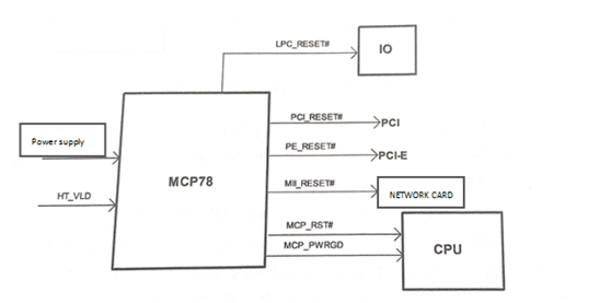
The working principle of the reset of the nVIDIA single-bridge MCP78 chipset motherboard is shown in figure 1.

Fig. 1 working principle block diagram for reset of nVIDLA single bridge MCP78 chipset motherboard.
1. The main board power-up circuit works, through the power supply circuit step-down to generate memory power supply, bridge power supply, CPU power supply and bus power supply.
2. Bus power supply through circuit conversion to the HT_VLD bus voltage good signal to the bridge, the bridge sends out MCP_PWRGD signal to the CPU, indicated that the main board power supply is normal.
3. The bridge issues the LPC_RESET# reset IO chip, the PCI _ RESET# reset PCI slot, the PE_RESET# reset PCI-E slot, the M11_RESET# reset Nic chip, and finally the MCP_RST reset CPU.
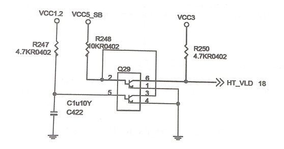
The HT_VLD signal circuit generates power from the VCC 1.2 bus to the 5-pin Q29 via the resistor R247, controls the 3-pin and 4-pin internal Triode on, and lowers the 2-pin voltage so that the 6-pin and 1-pin internal Triode cutoff, The HT_VLD is sent to the bridge via the R250 pull-up for 3.3 V, indicating that the bus is powered properly.

Fig. 2 HT_VLD signal generation circuit.


没有评论:
发表评论