2019年10月31日星期四

FISO fiber optic sensor detects temperature changes in food in microwaves

The MWS Microwave Workstation is designed to perform temperatures measured in a microwave oven equipped with a turntable. Fiber optic sensing technology is completely resistant to microwave energy and provides accurate and reliable measurements in the microwave cavity.

The microwave workstation is equipped with FISOCommander workstation software for complete sensor and results management. Microwave workstations meet the needs of most food developers and testers. With its unique patented technology, the Microwave Workstation provides the absolute accuracy of measuring the absolute cavity length of the FISO Fabry-Perot fiber optic sensor, providing highly accurate and reliable measurements.


The Microwave Workstation is compatible with all FISO fiber optic sensors, including strain, pressure, temperature, displacement, refractive index, force and loading. FISO's fiber optic sensors are fully resistant to RF and microwave radiation with high temperature handling and intrinsic safety. The sensor is also designed to withstand harsh and corrosive environments.

Microwave Work Station enables automatic data collection and seamless data exchange with standard spreadsheet programs such as Microsoft Excel or Lotus 1-2-3. The data includes test sessions for temperature and pressure readings collected during this period. The picture of the sample being tested and the location of the sensor can also be saved in the test file. This valuable information is easily categorized and retrieved at any time for comprehensive data analysis and comparison.

The microwave workstation includes a microwave oven with turntable, a fiber optic rotating device for temperature measurement, FISOComman der Workstation software, all necessary wiring and a comprehensive instruction manual.
main feature:
1. Up to 16 Fibre Channel
2. Sequential measurement
3. Turntable microwave oven
4. Collect and save data, spreadsheet compatible formats
5. Rugged, easy to use fiber optic sensor
6. Fully immune microwave energy
Main application:
1.Food development
2. Food packaging development
3. Microwave food testing
4. Microwave food processing
5. Cookware design
6. Microwave oven design and testing
7. New material research
8. Microwave and RF related applications

The FISO fiber optic sensor uses an interference principle that is ideal for environments where the food industry environment and dielectric sensors are not working. The FISO sensor and its corresponding signal conditioner can form a complete fiber optic sensing system. An interferometric sensor (FPI) generally consists of two opposite mirrors, and the space separating the two mirrors is called the length of the cavity (or void). The light reflected into the FPI is wavelength modulated and is exactly the same length as the cavity. The strain, temperature, displacement or pressure is converted as a function of the length of the cavity by a precisely designed FPI. The principle of the FISO sensor is that when the beam reaches the end of the fiber, it enters a conical medium, causing reflections on the upper and lower surfaces, which in turn cause interference of light. The position at which the reflection occurs is different, and the corresponding optical path difference is also different. When the lateral movement of the chevron medium indicates a change in displacement, this displacement change will be detected and converted by the FP cavity. Because the FISO sensor is completely resistant to electromagnetic, microwave and radio frequency interference, multi-channel online real-time detection of the differences and changes in the temperature of the food in the microwave provides reliable and accurate data for studying the moisture and content of food at different temperatures. Here, the main fiber optic temperature sensor imported from Canada - FOT-L-BA and fiber optic temperature sensor - FOT-L-SD, these two fiber optic temperature sensors are very suitable for measuring temperature in extreme environments, this extreme The environment includes low temperature, nuclear environment, microwave and high intensity RF. The FOT-L combines all the great features you'd expect from an ideal sensor body. Therefore, such sensors provide high accuracy and reliable temperature measurement even under extreme temperatures and adverse conditions.

This article is from Allicdata Electronics Limited.

2019年10月26日星期六

Monolithic digital-to-analog converter and hybrid digital-to-analog converter

This article briefly introduces Monolithic/Hybrid Digital to Analog Converters
DIGITAL TO ANALOG CONVERTERS,both of them have been designed for four inputs. But, if the number of inputs is more than four, the combination of output becomes more than 16. This makes the circuit more complex and the accuracy of the circuit reduces. Therefore, in critical and complex applications, a monolithic/hybrid D/A converter IC must be used. With the help of binary-weighted resistor, and R  and 2R resistor methods, 8-bit,10-bit, 12-bit, 14-bit, and 16-bit D/A converters can be designed with a current output, voltage output, or both current and voltage outputs.
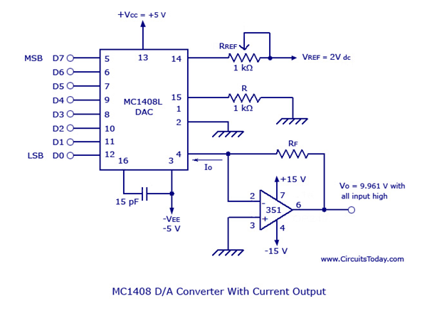
The most commonly used 8-bit D/A converter is MC 1408 which has a current output that can be converted to a voltage type using a current to voltage converter op-amp. The design along with the current to voltage converter is shown in the figure below.
image.png
MC 1408 Digital to Analog Converter
V0 = Vref/Rref *(RF)*{D7/2 + D6/4 + D5/8 + D4/16 + D3/32 + D2/64 + D1/128 + D0/256}
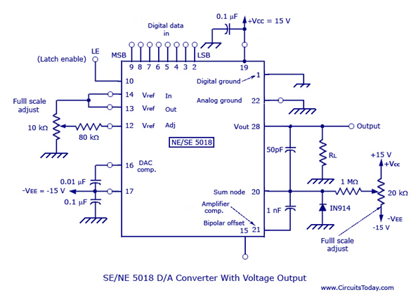
SE/NE 5018 is a typical 8-bit D/A converter with voltage output. The figure is shown below.
image.png
SE-NE 5018 Digital to Analog Converter
In the figure, the SE/NE 5018 circuit is configured for uni-polar output (0V to 10V). For 12 bits of resolution as well as current and voltage outputs, hybrid D/A converters such as DATEL DAC-H2 series is used.
For the correct selection of the D/A converter out of the lot, some important specifications of the converter must be known.
This article is from Allicdata Electronics Limited. Reprinted need to indicate the source.

2019年10月18日星期五

Hitachi integrates AI technology into car stereo cameras to enhance nighttime pedestrian detection

Hitachi Automotive Systems said it has applied artificial intelligence (AI) technology to stereo cameras, which are designed for automotive automatic braking. The camera uses hundreds of thousands of data as "teacher data" to achieve night pedestrian detection. At present, various competitors are developing sensors that support AI. Hitachi Automotive Systems will supply this new sensor to Suzuki Motor Co., Ltd. in order to lead the commercialization of AI sensors.

According to the company, the new sensor's performance is much better than its competitors' products, able to detect pedestrians at night, and then the car can automatically brake, more braking performance than vehicles equipped with Israel Mobileye's main image processing chip EyeQ3 it is good.

Previously, Hitachi’s cameras were “rule-based” to identify objects, ie developers needed to set conditions manually, as did other companies’ products. However, the "rule-based" approach complicates conditions and makes it difficult to support nighttime object detection. This time, Hitachi uses machine learning technology to effectively find conditions in large amounts of data.

In general, a stereo camera uses two left and right cameras to take two images, and then uses the parallax between the two images to detect the shape of the object and the object located in front of the vehicle, and then use pattern recognition to determine the detected object. Whether it is a pedestrian. The stereo camera of Hitachi Automotive Systems will use machine learning to perform image recognition.

Hundreds of thousands of "teacher data" are stored in the image processing microcomputer of the new camera, and then the image taken by the camera is compared with "teacher data" to determine whether the object is a pedestrian. Previously, the stereo camera of Hitachi Automotive Systems used the normal pattern recognition method, which uses multiple images for judgment.

Even if the pedestrian is only illuminated by the headlights of the car or the entire body of the pedestrian can be seen, and the brightness of each body part is different, the camera uses machine learning, which is easier to detect than the traditional pattern recognition method.

The Hitachi Automotive System also increases the dynamic detection range of the CMOS sensor, reducing the F value of the lens (the smaller the F value, the larger the aperture) and doubling the sensitivity of the camera. Thanks to its dynamic range of motion detection, the camera captures both bright and dark objects. And because the F value is smaller, the camera is more likely to find pedestrians in the dark.

When machine learning techniques are applied to image recognition processing, the amount of data that needs to be processed is increased. In order to solve this problem, the Hitachi Automotive System has modified the microcomputer of the stereo camera to improve its performance. The previous stereo camera used three microcomputers for image processing, image recognition, and vehicle control. The new stereo camera of Hitachi Automotive Systems integrates only two microcomputers for image processing and image recognition. Then, the microcomputer for image recognition is upgraded from a single core to a dual core. As the number of cores increases, the microcomputer can not only use machine learning technology, but also improve the processing speed of image recognition.

2019年10月14日星期一

Integrated passive components in micromodule SIP

Integrated passive devices are nothing new in our industry – they have been around for a long time and are well known.In fact,Analog Devices has produced such components for the market in the past.Careful design management of trace parasitics,device compatibility,and board assembly considerations is required when the chipset includes separate discrete passive components or integrated passive networks as part of it.While integrated passive devices continue to play an important role in the industry,their most important value can only be realized when they are integrated into system-in-package applications.

A few years ago,ADI began rolling out a new integrated passive technology program (iPassivesTM).Through this program,ADI aims to provide passive components such as diodes, resistors,inductors,and capacitors to cover signal chain design more broadly while overcoming the limitations and complexities of existing passive component methods.The need for a more complete solution with an efficient space size from ADI's customer base has also driven this program.From a designer's point of view,iPassives can be viewed as a flexible design tool that can design system solutions with best-in-class performance and robustness in a very short development cycle.ADI has a number of signal conditioning ICs,and our unique silicon manufacturing process enables these ICs to achieve superior performance.ADI can leverage the diversity of its existing products to produce plug-and-play systems with superior performance characteristics without the need to develop highly complex integration processes.Integrate passive technology with all of these existing technologies in a highly customizable network and package it with system-in-package technology to create fully certified,tested and characterized μModule® devices.Systems that previously used board-level solutions can now be simplified to a single device.From our customer's point of view,they now have a complete solution with outstanding out-of-the-box performance,reduced development cycles and cost savings,all in a very compact package.

Passive technology

Now let's briefly review the basics and recall what passive components are. Passive components are devices that do not require a power supply, and their relationship between current and voltage is relatively simple. These components include resistors, capacitors, inductors, transformers (ie, effectively coupled inductors), and diodes. Sometimes the relationship between current and voltage is very simple, just as the current in a resistor varies linearly with voltage. For diodes, there is also a direct relationship between current and voltage, but this relationship is an exponential relationship. In inductance and capacitance, this relationship is the transient dependence of current on voltage. Table 1 shows the formula for defining these relationships for the four basic passive components:

Table 1. Basic formulas for the main passive components
Using integrated passive components in the micro-module SIP

Passive devices can be used alone or in series or in parallel, for analog signal processing (RLC for amplification, attenuation, coupling, tuning and filtering), digital signal processing (pull-up resistors, pull-down resistors and impedance matching resistors), EMI Suppression (LC noise suppression) and power management (R for current detection and limiting, LC for energy accumulation) is an important part.

Limitations of discrete components

In the past, passive components were discrete, meaning that they were fabricated separately and connected in the circuit by wires or power rails on a printed circuit board (PCB). Over time, they evolved along three paths: smaller size, lower cost, and higher performance. These developments are now mature and optimized, but the footprint size and height dimensions mean that discrete passive components always limit the effort to reduce the size and size of the overall solution. Passive devices typically account for more than 80% of the bill of materials in an application, accounting for approximately 60% of the board area and approximately 20% of the total component expense. These factors combine to create very complex inventory control and storage challenges.

By its very nature, discrete devices are individually processed components. Although there may be ways to ensure that components are selected from certain process batches, each component is still highly unique. However, this is a significant disadvantage when a very matched component is required. For devices that need to be matched, the uniqueness and variability between components can cause errors, which can reduce the circuit performance at time zero. In addition, this performance degradation is always getting worse during the operating temperature range of the circuit and during its lifetime.

Another disadvantage of discrete passive components is that the assembly and routing of individual components is time consuming and takes up a lot of space.These components are connected using a soldering process and are typically assembled through via or surface mount packaging (SMT).Through-hole is an older assembly technique that inserts a leaded device into the hole in the PCB,any excess lead length will be bent and cut,and the device leads are connected to the PCB interconnect by wave soldering.rail.Surface-mount packages help achieve smaller passive components.In this case,the mounting connection pattern is etched on the PCB,the solder paste is overlaid on the pattern,and then the placement machine is used to position the SMT component.The PCB is then subjected to a reflow process (where the solder paste liquefies and establishes an electrical connection),and upon cooling,the solder paste solidifies and mechanically connects the SMT component to the PCB.The main problem with these two assembly techniques is that the welding process can be very unreliable,and this is becoming more and more worrying in industries where the target of defects is in parts per million.Several factors are important in ensuring solder joint reliability:the actual composition of the solder paste (now basically lead-free,so reliability is reduced),mechanical stability in the reflow process (mechanical vibration can make solder joints) Dry),the purity of the solder paste (any contaminants can have a negative impact on the reliability of the solder joint),as well as the time and temperature in the reflow process.The speed at which the solder paste is heated,the uniformity of the actual temperature and temperature,and the time the solder paste is heated are critical.Any of these changes can cause damage to the connection pads or vias,or it can cause mechanical stress on the device that can cause failures over time.

Another limitation of using passive components on the PCB is that the traces need to be long due to their distribution throughout the board.This may introduce parasitic parameters that are not counted,thereby limiting performance and result repeatability. Typically,PCB traces have a length and capacitance of approximately 1 nH/mm self-inductance,depending on the line width and distance from nearby traces.The tolerance of PCB traces leads to variations in parasitic parameters,so it not only brings parasitic damage,but they are still unpredictable.Shrinking tolerances on PCBs increases costs.

Passive devices also provide a number of potential contact points with the outside world that can be subject to ESD events through manual processing or machine processing.Again, this can have adverse effects and risks on overall reliability and robustness.

Advantages of integrated passive components

Before delving into the advantages of integrated passive devices compared to discrete passive devices,we first outline the origins of integrated passive devices.Integrated circuits now contain many transistors (in fact,millions) that are connected to each other by fine metals. For analog applications,the industry has also developed special processes such as DACs and ADCs that include passive components such as resistors and capacitors in addition to transistors.In order to achieve the performance required for these sophisticated analog applications,very high quality passive components have been developed.These high quality passive components are used to build integrated passive components.Just as integrated circuits contain many transistors,integrated passive devices can contain many high-quality passive components in a very small package. Like integrated circuits,integrated passive devices are fabricated on large-area substrates (wafers) while generating multiple passive networks.

One of the most compelling advantages of integrated passive components compared to discrete passive components is the ability to achieve precise matching.When manufacturing an integrated passive network,all components within the network are manufactured simultaneously under the same conditions,have the same material,and are basically in the same location due to the compact network. Passive components fabricated in this manner are more likely to have an excellent match than discrete passive components.To illustrate this,let's assume that there is an application that requires two matched resistors.These resistors are fabricated on a circular substrate such as a silicon wafer,as shown in Figure 1.Due to subtle process differences,such as the thickness of the resistive film,the chemical nature of the film,the contact resistance, etc.there will be a certain difference in resistance in the same batch,and the difference value will be larger in multiple batches. In the example shown in Fig.dark green indicates that the resistance is at the high end of the tolerance range,and yellow indicates that the resistance is at the low end of the tolerance range.For a standard discrete device,either of the two resistors may come from a different manufacturing lot, as shown by two separate resistors in red.The range of tolerances that can be observed between these two discrete resistors may be the tolerance of the entire process,so the matching is poor.For special ordering restrictions,it is possible to select the two discrete resistors from the same batch,as shown by the two separate resistors in blue.

The observable tolerance between these two resistors will only be the tolerance range within the same batch.Although the match between these two resistors will be better than in the case of random discrete devices,there may still be some degree of mismatch.
Finally,for integrated passive devices,the two resistors come from the same chip,as shown in Figure 1 black.The only observable tolerance between these two resistors is the tolerance range within the same die.Therefore,the match between these two resistors will be excellent.In addition,other techniques and other methods using a crossed quadrilateral layout can further severely limit the diffusion between the two resistors to achieve optimum matching of the components.Matching between integrated passive components is not only better at time zero than discrete passive components,but also maintains better matching over temperature,mechanical stress and lifetime over time due to their well-coupled manufacturing.recording.

Using integrated passive components in the micro-module SIP

The individual components in the integrated passive device are placed closely together (actually in the micron range),so interconnect parasitic parameters such as wiring resistance and inductance can be kept to an extremely low level.On the PCB,interconnect parasitics may change due to trace tolerances and component placement tolerances.Because of the lithography process used in the manufacturing process,interconnect tolerances and component placement tolerances using integrated passive components are small.In integrated passive devices,not only are the parasitic parameters very small,but these few parameters are predictable and therefore highly reliable.

The miniaturization of passive networks by integrating passive components brings the advantages of small size directly to the board.This directly reduces board cost and allows for more functionality and higher performance in a smaller footprint.When using integrated passive components,building a multi-channel system becomes more practical.

Another significant advantage of integrated passive components is the robustness around their entire wiring network.Integrated passive components are essentially forged together in a complete unit,sealed with glass,and then further protected by a robust plastic package without the need for extensive solder connections.In integrated passive networks,there is no problem with solder joint drying,corrosion or component misalignment.

Another advantage of the excellent performance of the integrated passive network seal is that the number of exposed nodes in the system is greatly reduced. As a result, the likelihood of system damage due to accidental short circuits or electrostatic discharge (ESD) events is significantly reduced.

Maintaining and controlling the inventory of components assembled on any board is a very complex task.Integrated passive components contain multiple passive components in a single device,greatly reducing the customer's bill of materials burden and reducing the cost of ownership.Customers get fully tested and fully validated integrated passive networks.This means that the output of the final board construction is improved,which not only saves further costs,but also improves the predictability of the supply chain.

Use ADI's Integrated Passives (iPassives)

As mentioned earlier,high-quality passive components have been at the heart of the circuit performance that ADI has achieved over many years.During this time,the range of passive components continues to expand and quality continues to improve,and the integrated passive device portfolio now includes a large number of components.The integrated passive device uses a modular process,which means that the process steps required to produce a certain type of passive device need to be performed only when specific components are required.The construction of the iPassives network basically requires only the necessary process complexity,no more and no less.As shown in Figure 2,there are many passive building blocks to choose from,and building an integrated passive network is as simple as assembling the required components together.

Using integrated passive components in the micro-module SIP

As mentioned earlier in this article, integrated passive devices have many advantages over discrete passive devices. ADI has further enhanced these advantages by using them in μModule devices. These modules take advantage of the capabilities of various integrated circuits. These circuits are manufactured through a tailor-made process that provides enhanced performance that cannot be achieved by any other single process. ADI is using iPassives to connect these integrated circuits together to build a complete precision signal chain in a single device. The two μModule device examples in Figure 3 include data converters, amplifiers, and other components that are combined by a passive gain and filter network built with integrated passive components.

Using integrated passive components in the micro-module SIP

ADI produces highly customizable precision signal conditioning systems.Using a reusable approach from a large portfolio of field-proven IC products and combining it with the versatility of iPassives,the development cycle time and cost are significantly reduced. This decision provides customers with a huge advantage,allowing customers to use their most advanced performance to get to market faster and more efficiently.

in conclusion

At first glance,using integrated passive devices may only be slightly more advantageous than other more mature methods. However,the practical advantages are even more pronounced.ADI's adoption of iPassives not only redefines the achievable functions,but also redefines speed,cost and design size to make it more beneficial to customers.
2019年10月12日星期六

What is the parameter of the inverter

The parameter setting of the inverter is very important during the commissioning process. Many users who use the inverter for the first time, because they do not fully understand the meaning of these parameters, plus the listed setting parameters are more, there are some overwhelming how to set the parameters of the inverter. For these users, you need to master the basic knowledge of the inverter parameter setting: which parameters need to be set before the test run; which parameters need to be adjusted during operation and the appropriate range of adjustment; how to prevent the frequency conversion caused by improper parameter setting during the debugging process Damage to the device and so on.

  • Classification of inverter parameters
1, do not have to adjust the parameters that can maintain the factory settings
2. pre-set parameters before commissioning
3. parameters that need to be adjusted during trial operation

  • Commonly used inverter parameters are
1. control method:
2, the minimum operating frequency:
3, the highest operating frequency:
4, carrier frequency:
5, motor parameters:
6, frequency hopping:
7, acceleration and deceleration time
8, torque boost
9, electronic thermal overload protection
10, frequency limit
11, bias frequency
12, frequency setting signal gain
13, torque limit


This article is from Allicdata Electronics Limited which offer electronic components, semiconductors, antennas, capacitors, connectors, diodes, transistors, ICs, resistors
For more product information, please go to the website to get it.

2019年10月11日星期五

Basic knowledge of semiconductor diodes, do you know?

In recent decades, electronic technology has developed rapidly and has become more and more widely used. It has become an important part of modern science and technology. What is electronic technology? Simply put, electronic technology is the science and technology to study electronic devices, electronic circuits and their applications. Learning analog electronics will lay the foundation for us to further study the content in the field of electronic technology and the application of electronic technology in the profession.
Starting with the formation of a pN junction, the semiconductor diode and its application are known.
1. Intrinsic semiconductor: pure crystal structure covalent bond free electron hole (pair in appearance) ie carrier (2 species) [hole current electron current]
Features: high resistivity, electrical conductivity with temperature changes
2, doped semiconductor
a: N-type semiconductor: doped with a pentavalent element impurity (donor impurity), and the free electron is a multi-sub (the majority carrier is called a multi-sub).
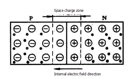
image.png
Hole is the minority
The concentration of the multiplier is related to the concentration of the impurity incorporated rather than the temperature, and the concentration of the minority is related to the temperature.
b: P-type semiconductor: doped with trivalent element (boron) acceptor impurity, hole is multi-sub, free electron is minority
If the impurity concentration of the pentavalent element is more than the concentration of the trivalent impurity, the P type can be turned to the N type.
3. Formation of PN junction
Multi-sub-concentration on both sides - multi-sub-diffusion - forming an internal electric field - hindering multi-sub-motion - enhancing the drift of the few children - drifting and spreading to achieve dynamic equilibrium - forming a PN junction
Note: Due to the large difference in multi-sub-concentration between the N-type semiconductor and the P-type semiconductor on both sides of the interface, the multi-substrate on the P-type semiconductor side is a hole, and its concentration is much larger than that of the N-type semiconductor; N-type semiconductor The multiple molecules on the side are electrons, and their concentration is much larger than that of the P-type semiconductor side. This concentration difference causes the multiple sub-diffusions to reach each other through the interface, and recombines with the other's multiple sub-subjects, so that the P-region forms a thin film layer with no holes and only negative ions near the interface; the N region forms a lack near the interface electron, only a thin layer of positive ions.
4. Unidirectional conductivity of PN junction
a: forward bias of the PN junction P—the positive pole of the power supply N—the negative pole of the power supply. The external electric field weakens the internal electric field, the dynamic balance breaks, the multi-sub-diffusion motion is strengthened, and the minority carrier drift motion is weakened, forming a forward current—the PN guide through
b: reverse bias of the PN junction P - negative power supply N - positive power supply, then PN cutoff
5. Relationship between current and voltage on pN junction
There is a relationship such as IF=Isexp(-eVF/kT), where -e is the electron charge; k is the Boltzmann constant; T is the absolute temperature; Is is the reverse saturation current, and the forward voltage U>0, i=Isexp(U/ut); Reverse voltage U<0, i=IS (I is independent of U).
If you want to know more, our website has product specifications for the semiconductor diode, you can go to ALLICDATA ELECTRONICS LIMITED to get more information

2019年10月10日星期四

What is the logic of digital electronics?

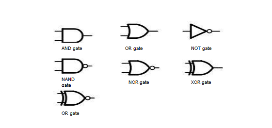
In the digital circuit design, the logic gate is the most basic arithmetic unit, and the AND gate, OR gate and NOT gate are the most basic logic gate units, but the logic used in the actual design is often much more complicated than, but They can all be implemented using a combination of AND, OR, and NOT. For example, NAND, NOR, XOR, and OR gate. The graphical symbols of these logic gates are as follows:
image.png
How to build a circuit utilizing a door unit?
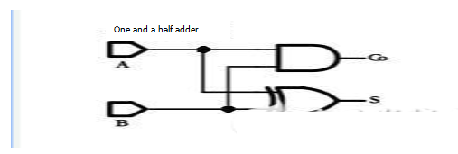
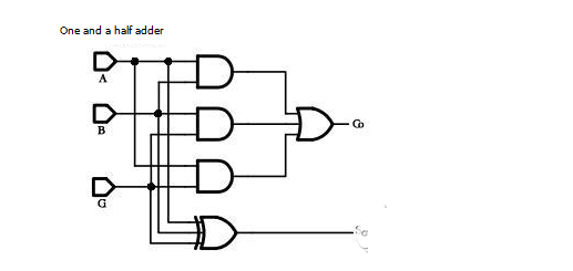
The circuit built by the gate unit is called the gate circuit. According to a certain logic relationship, different gate units are connected to realize the logic function we need. This is the purpose of digital circuit design. Here are two examples of using a logic gate unit to build a half adder and a full adder gate circuit:
image.png
The figure above is a half-adder circuit constructed by an AND gate and an XOR gate, where A and B are the input signals of the half adder, S is the result output of the half adder, C is the carry input of the half adder.
image.png
The above figure is a full adder circuit built by the logic gate unit. A and B are the input signals of the full adder, Ci is the carry input signal of the full adder, S is the full adder result output, and Co is the  carry output of the full adder.

Why can I implement the addition function? The following is a simple analysis of the principle of the addition function of the above two gate circuits. First, explain the difference between the half adder and the full adder: the half adder only adds the input signals A and B regardless of the carry; the full adder adds the carry Ci in addition to the A and B additions.

Among them, the half adders are added, and only when A and B are both 1, the addition will generate a carry, so Co=A&B. When both A and B are 0, the addition result S=0. Only one of A and B is 0 and the other is 1, the addition result S=1, so S=A^B.

The operation of the full adder is a bit more complicated. When one or three of the three inputs A, B, and Ci are 1, the addition result S=1, otherwise S=0, so S=A^B^Ci; When any two or three of the three inputs A, B, and Ci are 1, the addition will result in a carry of Co = 1, otherwise Co = 0, so Co = A & B | A & C | B & C.

If you want to know more, our website has product specifications for logic gate circuit, you can go to ALLICDATA ELECTRONICS LIMITED to get more information

2019年10月9日星期三

Pin diagrams of infrared receivers and amplifier circuits, where are the differences, how should they be distinguished?

The principle of the infrared receiving head is that the infrared monitoring diode monitors the infrared signal, and then sends the signal to the amplifier and the limiter. The limiter controls the pulse amplitude to a certain level regardless of the distance between the infrared transmitter and the receiver. The AC signal enters the bandpass filter, the bandpass filter can pass the load wave from 30khz to 60khz, enter the comparator through the demodulation circuit and the integration circuit, and the comparator outputs high and low levels to restore the signal waveform of the transmitter.

The infrared receiving head is an integrated receiving head composed of an infrared receiving tube and an amplifying circuit. The amplifying circuit is usually composed of an integrated block and a plurality of resistors and capacitors, and needs to be packaged in a metal shielding box, so that the circuit is complicated and the volume is small.

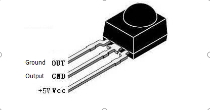
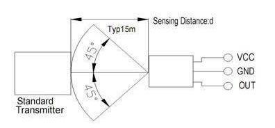
There are many types of infrared receivers, and the pin definitions are different. Generally, there are three pins, including power supply pins, grounding and signal output pins. The receiving head of the corresponding demodulation frequency should be selected according to the difference of the modulated carrier at the transmitting end.
image.png
Because the engineering process is to insert the board after spot welding, the project needs to understand the pins of the infrared receiver to make the pins correctly pair the board. So how do you identify the three pins of the infrared receiver?
image.png
There are generally two methods, the first one is the simplest, let the infrared receiver supplier provide the model specification, through the specification to distinguish the pins of the receiver. The other is to use the mechanical meter to measure the resistance of the two pins, find the one with the lowest resistance of the two pins. At this time, the watch stick should not move. The red watch stick is connected to Vcc, the watch stick is grounded, and the other pin is the signal pin(IR).

The three pins of the infrared receiver are GND, Vcc, and Out pins, which are ground, power, and signal outputs. Different types of infrared receivers have different pinouts.
image.png
The gain of the internal amplifier of the infrared receiving head is very large, which is easy to cause interference. Therefore, the VCC (voltage) PIN pin and the GND (ground) pin of the receiving head must be added with a filter capacitor. The expert test test is generally performed on a 47uf ceramic capacitor ( Note: Adding a capacitor to a 100uf or 20UF capacitor will cause the receiver to receive a short distance.

Infrared integrated receiving head: The infrared receiving head is generally a receiving, amplifying and demodulating integrated head. After the infrared signal is demodulated by the receiving head, the difference between the data “0” and “1” is usually reflected in the length of the high and low level or During the signal cycle, when the MCU decodes, the output pin of the receiving head is usually connected to the external interrupt of the MCU, and the time of the external interrupt interval is judged by the timer to obtain the data. The point is to find the difference in waveform between the data "0" and "1". The output can be connected to CMOS and TTL circuits. This type of receiver is widely used in air conditioners, TVs, VCDs and other electrical appliances.
If you want to know more, our website has product specifications for the infrared receiver and the amplifier circuit, you can go to ALLICDATA ELECTRONICS LIMITED to get more information

What is the development status and trend of led display?

  Over the past few years, with the further release of the market, the entire LED display industry has regained its vitality, and market com...