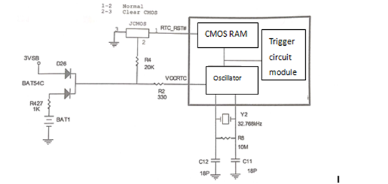
Because the main board manufacturer's circuit design is different, the CMOS circuit will be different. The main board CMOS circuit mainly consists of CMOS random access memory, real-time clock circuit (RTC circuit), jumper, south bridge chip, battery and power supply circuit, etc.

Fig. 1 composition of the CMOS circuit.
When the power supply is not connected to 220V, the positive pole of the battery is sent to the positive pole of the Schottky diode BATS4C through the resistor R427, and output from the negative pole. When connected to 200V, the ATX power supply output 5VSB standby power supply, through the main board step down to get the 3VSB standby power supply, send to the BAT54C positive pole, from the negative pole output, through the resistor R2 renamed VCCRTC to the South Bridge real-time clock circuit of the oscillator power supply. The other is sent to the two feet of the JCOMS jumper through the resistor R4, and pulled by the jumper cap to get the high-level RTC _ RST# signal to the South Bridge, and reset the CMOS random access memory inside the South Bridge. After the oscillator is supplied, the external Y _ 2 crystal oscillator is supplied, and the crystal oscillator starts to generate 32.768kHz frequency to the south bridge. When the VCCRTC,RTC _ RST# and 32.768kHz frequencies of the South Bridge are obtained, the internal CMOS RAM begins to work.
The role of CMOS RAM is to store important information such as the date and time of the system, the parameters of the memory setting on the motherboard, the configuration of the hard disk of the current system and some parameters set by the user, which are initialized by the BIOS to the system self-test at the time of power-on.


没有评论:
发表评论