2020年11月19日星期四

How does an infrared proximity sensor work?

 This article describes the characteristics of the sensor.

A new generation of young consumers has changed their decades of audio-visual habits. Earphones were worn only when needed, but now the introduction of true wireless (TWS) earbuds has changed this habit: Now, users do n’t even listen They wear earbuds all the time, just like people wear watches all the time, and TWS earbuds are very comfortable, convenient and unobtrusive.

Industry analysts predict that the market will grow at a compound annual growth rate of 27% by 2023, when TWS is expected to surpass all other types of wireless and wired headsets in sales.

Facing such rapid growth, earphone manufacturers will inevitably face fierce competition, and the choice of consumer products will be affected by important parameters such as audio quality, comfort and reliability.

Another crucial factor will be battery life to maintain longer battery life. One way to reduce power consumption is to make sure that the earbuds automatically stop playing when you remove them from your ears, and turn them on again when you insert them.

This requires short-range proximity sensing. In mobile phones, an infrared (IR) proximity sensing module detects when the phone is held on the user's face during a voice call, which can turn off the display. The following article describes how this technology can be adapted to small space TWS earbuds and how to reliably detect whether the earbuds are inside or outside the ear.

Working principle of infrared proximity detection

The basic operation of infrared proximity sensor is shown in Figure 1.

Figure 1: IR proximity sensor detects light reflected from nearby objects

It contains two main components:

An invisible infrared emission source that emits modulated light pulses. Ideally, the emitted power should be concentrated in a narrow band.

A photodiode (light sensor) with peak sensitivity at a wavelength that matches the peak intensity of the transmitter.

By strictly controlling the operating wavelength of the system and modulating the pulse, the sensor system can be protected from noise. The noise mainly includes interference from external infrared energy sources (such as sunlight) and internal reflection (crosstalk) from the module housing to the optical system. other parts. When the emitted infrared light hits the target in the range, it will be reflected on the photodiode. The photodiode converts the measured infrared energy into a digital value, which will increase proportionally as the target approaches.

In TWS earbuds, the proximity sensor is usually configured to trigger a detection signal when the object (in this case, the user's ear is open) is within 3 mm, and release the signal when the nearest object is within 10 mm. . Reliable proximity detection requires sufficient signal-to-noise ratio (SNR). To determine the SNR, the manufacturer needs to calculate the difference between the detection threshold and the release threshold count divided by the baseline jitter value (when there are no objects in the range):

       (Average detection count value) – (Average release count value)

       (Jitter count value)

       Generally, when this ratio is> 4, the SNR is considered acceptable.

Why every mW is important

Proximity sensors can reduce power consumption by detecting when the earbuds are removed from the ear and entering standby mode, but the sensor itself consumes energy: most of the sensor's energy consumption is attributed to the infrared transmitter. Fortunately, earplug designers can use one of two techniques to limit the power consumption of the sensor. The first is by controlling the launch cycle. In ams' integrated proximity sensor module TMD2635, the duty cycle configuration is easy to control (see Figure 2).


Figure 2: Pulse timing of a single proximity event in the TMD2635

The number of times the emitter is pulsed (PPULSE) and the duration of the effective drive current (PPULSE_LEN) of each pulse can be adjusted. The power consumption is proportional to the number of pulses and the pulse length. You can increase or decrease the total time of a PRATE, which is the main method for controlling the duty cycle. System designers can also introduce latency (PWTIME) between proximity measurement cycles.

The second way to control the duty cycle is through a signal generated at the application software level. Here, the host processor can be programmed to cycle the active / inactive state of the sensor in a polling or interrupt-driven manner. The polling method enables the host MCU to precisely control the system timing. Here, the proximity sensor is usually in a static low power state. The host microcontroller periodically issues commands to wake up, take a proximity measurement, and then return to a static state. In this polling mode, the designer can configure an optimal duty cycle that uses minimal power while providing an acceptable wait time, i.e. the delay between the user inserting / removing the earbud and the sensor detection event .

 In the interrupt-driven method, the MCU wakes up the sensor, reads its previous sample, and then makes it free-running. When the next data event occurs, the sensor sends an interrupt signal to the host, and then automatically goes to sleep. The advantage of this interrupt-driven approach is that the designer can choose which type of event will generate an interrupt signal. This allows the system to offload many tasks from host firmware to sensors. Since the CPU in the host consumes power, offloading can save power. Therefore, when the TMD2635 performs its "sleep after interrupt" function, it will automatically disable its internal oscillator and enter a low power state.

The TMD2635's programmable threshold function is particularly useful for triggering an interrupt when an adjacent data event falls outside a preset range between the high count threshold and the low count threshold, which can be set to only after the count repeatedly exceeds the threshold window Triggering, this function and other interrupt filtering functions are implemented in the hardware of the TMD2635, thereby reducing the burden on the host processor.

It is worth noting that compared to polling, the timing in interrupt-driven mode is less deterministic, and the event-driven duty cycle will change with the response time of the host processor and the number of neighboring events. Unless a simplified preset is made, this variability makes accurate power calculations difficult, and benchmarking is often the best way to determine power consumption under dynamic operating conditions.

In interrupt-driven mode, the sensor spends most of its time in free-running idle mode, which typically consumes an average current of 30 µA, which consumes more power than polling, which typically consumes 0.7 µA only when the sensor is in sleep Of current.

In the module-based transmitter TMD2635 proximity detection system, a low-power vertical cavity surface emitting laser (VCSEL) can bring further advantages. Most infrared proximity sensors have an LED emitter, but VCSELs can provide higher electro-optic conversion efficiencies, typically ten times higher than LEDs. In addition, because the beam is very narrow and the angle of view is only 1 ° to 5 °, the light energy of all transmitters can be aimed at the target. As a result, compared to equivalent LED-based sensor systems, the total power consumption is significantly reduced, crosstalk interference is reduced, and SNR is higher.

  Save space

Compared with earlier devices, the latest IR proximity sensor module integrates VCSEL technology, which has a substantial improvement in power consumption. Sensor manufacturers are also adjusting their product designs to fit the tight space inside TWS earbuds while maintaining a high level of optical performance.

Figure 3 shows that the proximity sensor can take up very little space in the TWS earphone reference design developed by ams. The TMD2635 used in this design has a package size of 1mm x 2mm x 0.5mm (see Figure 4).


Figure 3: TWS Headphone Reference Design Based on TMD2635 Module


Figure 4: TMD2635 proximity detection module is very small, occupying only 1mm3

The biggest difficulty in making such a small device is the optical design: ensuring that the emitted and reflected beams have clear paths to and from the target, while limiting the effect of crosstalk on photodiode measurements. In TMD2635, ams achieves this by combining component miniaturization, precise assembly, and high-performance optical stacking (see Figure 5).


Figure 5: Side view of TMD2635

The holes above the plutonium emitter and photodiode are covered by a polycarbonate material that is highly transparent to infrared light. The via can be round (1.5 mm in diameter) or oval (1 mm x 2 mm), giving designers greater flexibility when placing the sensor in the earbud housing.

 In conclusion

The TMD2635 module combines configurable power management technology, efficient VCSEL transmitters and optical components, and now provides a way for designers to more easily integrate proximity sensing in a small space inside the earbuds while providing Reliable detection of headphone position. This module's laser transmitter's high optical efficiency and low sleep mode current help keep average power consumption at a very low level, helping earbuds manufacturers to extend their product life, even with batteries as small as 25 mAh.


If you want to know more, our website has product specifications for the sensor you can go to ALLICDATA ELECTRONICS LIMITED to get more information


2019年11月15日星期五

Commissioning car controller ST Stellar

    By STMicroelectronics PLS programmable logic simplifies software development and systems support, Stellar automotive microcontroller architecture for this powerful debugging, tracking and testing.
     As the combination of several new technologies on the chip, the chassis and the telephone-assist auxiliary system (ADAS) can be implemented with a power system that is controlled by a personalized microcontroller series "Star". With the six Arm Cortex R52, the first building block generated by the latest microcontrollers is also the core clock frequency of 400 MHz. Together with 16 MB of embedded phase change memory (PCM), it provides high multicore performance for real-time applications.
       Further, Stellar series also has a variety of security and protection features, including a hardware security module (HSM) function and a lock-step. Management software program for the separation and storage protection enhances the security and reliability features.
       The Stellar range meets the stringent requirements of the automotive electronics system ISO 26262 to ASIL-D safety standards. In addition, three floating-point Cortex-M4 cores and DSP extensions act as application-specific accelerators. Due to the long-term close cooperation with STMicroelectronics, PLS has been able to develop optimized debugging and tracking tools for the ST-Partner Program to develop members with the first home from the Stellar to be able to provide this complex automotive microcontroller architecture.
      With multi-core run control, UDE's specific features, you can use the built-in debug logic to synchronize start and stop of all cores or selected groups. Multi-core breakpoints that can be used in shared code simplify the debugging of complex applications. Such a breakpoint is always valid no matter which kernel is currently executing the code. In addition to support for the actual application kernel, UDE also allows debugging of hardware security modules integrated on the Stellar MCU. To this end, HSM can be integrated into multi-core operational control.
The optimized programming of phase change memory (PCM) implemented in the Stellar family of modules is achieved by means of the UDE Memtool flash programming tool integrated in              UDE. Phase change memory allows for faster, safer, and more accurate programming than traditional flash programming. In practice, this means, for example, that even a single byte can be written, whereas only the entire block could have been written before. Due to the nature of the PCM, the over-the-air software (SOTA) for this storage technology can be used particularly efficiently and reliably. The special features of UDE Memtool ensure the smooth support of SOTA.
For detailed analysis of multi-core applications at the system level, the UDE supports a wide range of trace capabilities for the CoreSight debug and trace scheme, where the arm is in the              Cortex-R52-core core of the Cortex-M4, and for the connection to the chip has been achieve.
The family of three devices UAD2pro, UAD2next and UAD3 + PLS universal access devices are also reliably debugged to the stellar microcontroller family via JTAG or arm-specific serial line debug (SWD) interfaces. It is ideal for capturing and storing large amounts of trace data while UAD3+, which is available on the Star MCU with up to 4 GB of trace memory in the special tracking POD for High Speed Serial Trace Port (HSSTP),

2019年11月12日星期二

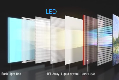
What is the structure of the LED screen?

      The difference between the LED screen and the OLED screen is not only a letter difference, but the imaging technology of the two is completely different.
      LED screen structure is more complicated

image.png

       LED screens and OLED screens have fundamental differences in the principle of illumination.
The full name of the LED is a light-emitting diode. Like the traditional semiconductor industry, LED display screens are a way of controlling the display of semiconductor light-emitting diodes. They are usually composed of a plurality of red light-emitting diodes, which are dominated by the display of lights, thereby realizing text, graphics, images, and animation. Display screen for various information such as video and video signals. Its process cost is high. In addition, LEDs can only be used in the form of point sources.
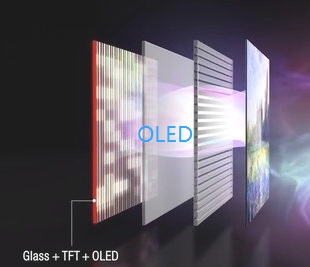
       OLED does not require a backlight, and the structure is lighter and thinner.

image.png 

        The OLED emits light by driving the organic film itself. OLED is a congenital surface light source technology, and the light emitted can be red, green, blue, white and other monochromatic colors, thereby achieving the effect of full color, belonging to a new principle of illumination. The reason why plasma technology, OLED technology and even the image quality of CRT technology in the early years are praised is mainly because they all have the characteristics of "self-illumination".

2019年11月4日星期一

The working principle of the nVIDIA motherboard circuit.

In the mainboard repair encountered nVIDIA motherboard is basically a single bridge, common also ASUS M2N68, M4N78 motherboard.

The nVIDIA motherboard automatically generates a clock signal internally after normal power supply and resets when the bridge receives the HT_VLD signal.

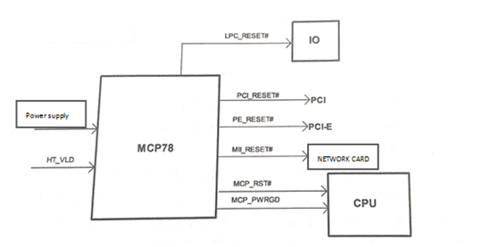
The working principle of the reset of the nVIDIA single-bridge MCP78 chipset motherboard is shown in figure 1.

 image.png
Fig. 1 working principle block diagram for reset of nVIDLA single bridge MCP78 chipset motherboard.

1. The main board power-up circuit works, through the power supply circuit step-down to generate memory power supply, bridge power supply, CPU power supply and bus power supply.

2. Bus power supply through circuit conversion to the HT_VLD bus voltage good signal to the bridge, the bridge sends out MCP_PWRGD signal to the CPU, indicated that the main board power supply is normal.

3. The bridge issues the LPC_RESET# reset IO chip, the PCI _ RESET# reset PCI slot, the PE_RESET# reset PCI-E slot, the M11_RESET# reset Nic chip, and finally the MCP_RST reset CPU.

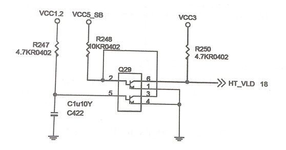
The HT_VLD signal circuit generates power from the VCC 1.2 bus to the 5-pin Q29 via the resistor R247, controls the 3-pin and 4-pin internal Triode on, and lowers the 2-pin voltage so that the 6-pin and 1-pin internal Triode cutoff, The HT_VLD is sent to the bridge via the R250 pull-up for 3.3 V, indicating that the bus is powered properly.
image.png
Fig. 2 HT_VLD signal generation circuit.


This article is from Allicdata Electronics Limited. Reprinted need to indicate the source.


2019年10月31日星期四

FISO fiber optic sensor detects temperature changes in food in microwaves

The MWS Microwave Workstation is designed to perform temperatures measured in a microwave oven equipped with a turntable. Fiber optic sensing technology is completely resistant to microwave energy and provides accurate and reliable measurements in the microwave cavity.

The microwave workstation is equipped with FISOCommander workstation software for complete sensor and results management. Microwave workstations meet the needs of most food developers and testers. With its unique patented technology, the Microwave Workstation provides the absolute accuracy of measuring the absolute cavity length of the FISO Fabry-Perot fiber optic sensor, providing highly accurate and reliable measurements.


The Microwave Workstation is compatible with all FISO fiber optic sensors, including strain, pressure, temperature, displacement, refractive index, force and loading. FISO's fiber optic sensors are fully resistant to RF and microwave radiation with high temperature handling and intrinsic safety. The sensor is also designed to withstand harsh and corrosive environments.

Microwave Work Station enables automatic data collection and seamless data exchange with standard spreadsheet programs such as Microsoft Excel or Lotus 1-2-3. The data includes test sessions for temperature and pressure readings collected during this period. The picture of the sample being tested and the location of the sensor can also be saved in the test file. This valuable information is easily categorized and retrieved at any time for comprehensive data analysis and comparison.

The microwave workstation includes a microwave oven with turntable, a fiber optic rotating device for temperature measurement, FISOComman der Workstation software, all necessary wiring and a comprehensive instruction manual.
main feature:
1. Up to 16 Fibre Channel
2. Sequential measurement
3. Turntable microwave oven
4. Collect and save data, spreadsheet compatible formats
5. Rugged, easy to use fiber optic sensor
6. Fully immune microwave energy
Main application:
1.Food development
2. Food packaging development
3. Microwave food testing
4. Microwave food processing
5. Cookware design
6. Microwave oven design and testing
7. New material research
8. Microwave and RF related applications

The FISO fiber optic sensor uses an interference principle that is ideal for environments where the food industry environment and dielectric sensors are not working. The FISO sensor and its corresponding signal conditioner can form a complete fiber optic sensing system. An interferometric sensor (FPI) generally consists of two opposite mirrors, and the space separating the two mirrors is called the length of the cavity (or void). The light reflected into the FPI is wavelength modulated and is exactly the same length as the cavity. The strain, temperature, displacement or pressure is converted as a function of the length of the cavity by a precisely designed FPI. The principle of the FISO sensor is that when the beam reaches the end of the fiber, it enters a conical medium, causing reflections on the upper and lower surfaces, which in turn cause interference of light. The position at which the reflection occurs is different, and the corresponding optical path difference is also different. When the lateral movement of the chevron medium indicates a change in displacement, this displacement change will be detected and converted by the FP cavity. Because the FISO sensor is completely resistant to electromagnetic, microwave and radio frequency interference, multi-channel online real-time detection of the differences and changes in the temperature of the food in the microwave provides reliable and accurate data for studying the moisture and content of food at different temperatures. Here, the main fiber optic temperature sensor imported from Canada - FOT-L-BA and fiber optic temperature sensor - FOT-L-SD, these two fiber optic temperature sensors are very suitable for measuring temperature in extreme environments, this extreme The environment includes low temperature, nuclear environment, microwave and high intensity RF. The FOT-L combines all the great features you'd expect from an ideal sensor body. Therefore, such sensors provide high accuracy and reliable temperature measurement even under extreme temperatures and adverse conditions.

This article is from Allicdata Electronics Limited.

2019年10月26日星期六

Monolithic digital-to-analog converter and hybrid digital-to-analog converter

This article briefly introduces Monolithic/Hybrid Digital to Analog Converters
DIGITAL TO ANALOG CONVERTERS,both of them have been designed for four inputs. But, if the number of inputs is more than four, the combination of output becomes more than 16. This makes the circuit more complex and the accuracy of the circuit reduces. Therefore, in critical and complex applications, a monolithic/hybrid D/A converter IC must be used. With the help of binary-weighted resistor, and R  and 2R resistor methods, 8-bit,10-bit, 12-bit, 14-bit, and 16-bit D/A converters can be designed with a current output, voltage output, or both current and voltage outputs.
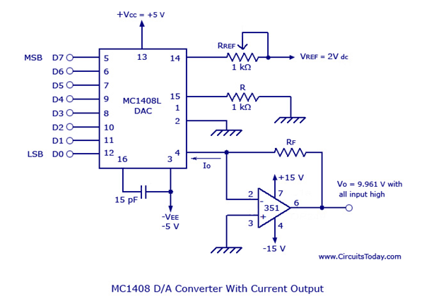
The most commonly used 8-bit D/A converter is MC 1408 which has a current output that can be converted to a voltage type using a current to voltage converter op-amp. The design along with the current to voltage converter is shown in the figure below.
image.png
MC 1408 Digital to Analog Converter
V0 = Vref/Rref *(RF)*{D7/2 + D6/4 + D5/8 + D4/16 + D3/32 + D2/64 + D1/128 + D0/256}
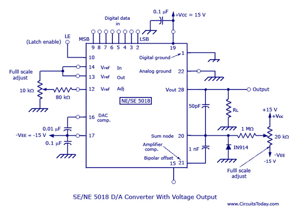
SE/NE 5018 is a typical 8-bit D/A converter with voltage output. The figure is shown below.
image.png
SE-NE 5018 Digital to Analog Converter
In the figure, the SE/NE 5018 circuit is configured for uni-polar output (0V to 10V). For 12 bits of resolution as well as current and voltage outputs, hybrid D/A converters such as DATEL DAC-H2 series is used.
For the correct selection of the D/A converter out of the lot, some important specifications of the converter must be known.
This article is from Allicdata Electronics Limited. Reprinted need to indicate the source.

2019年10月18日星期五

Hitachi integrates AI technology into car stereo cameras to enhance nighttime pedestrian detection

Hitachi Automotive Systems said it has applied artificial intelligence (AI) technology to stereo cameras, which are designed for automotive automatic braking. The camera uses hundreds of thousands of data as "teacher data" to achieve night pedestrian detection. At present, various competitors are developing sensors that support AI. Hitachi Automotive Systems will supply this new sensor to Suzuki Motor Co., Ltd. in order to lead the commercialization of AI sensors.

According to the company, the new sensor's performance is much better than its competitors' products, able to detect pedestrians at night, and then the car can automatically brake, more braking performance than vehicles equipped with Israel Mobileye's main image processing chip EyeQ3 it is good.

Previously, Hitachi’s cameras were “rule-based” to identify objects, ie developers needed to set conditions manually, as did other companies’ products. However, the "rule-based" approach complicates conditions and makes it difficult to support nighttime object detection. This time, Hitachi uses machine learning technology to effectively find conditions in large amounts of data.

In general, a stereo camera uses two left and right cameras to take two images, and then uses the parallax between the two images to detect the shape of the object and the object located in front of the vehicle, and then use pattern recognition to determine the detected object. Whether it is a pedestrian. The stereo camera of Hitachi Automotive Systems will use machine learning to perform image recognition.

Hundreds of thousands of "teacher data" are stored in the image processing microcomputer of the new camera, and then the image taken by the camera is compared with "teacher data" to determine whether the object is a pedestrian. Previously, the stereo camera of Hitachi Automotive Systems used the normal pattern recognition method, which uses multiple images for judgment.

Even if the pedestrian is only illuminated by the headlights of the car or the entire body of the pedestrian can be seen, and the brightness of each body part is different, the camera uses machine learning, which is easier to detect than the traditional pattern recognition method.

The Hitachi Automotive System also increases the dynamic detection range of the CMOS sensor, reducing the F value of the lens (the smaller the F value, the larger the aperture) and doubling the sensitivity of the camera. Thanks to its dynamic range of motion detection, the camera captures both bright and dark objects. And because the F value is smaller, the camera is more likely to find pedestrians in the dark.

When machine learning techniques are applied to image recognition processing, the amount of data that needs to be processed is increased. In order to solve this problem, the Hitachi Automotive System has modified the microcomputer of the stereo camera to improve its performance. The previous stereo camera used three microcomputers for image processing, image recognition, and vehicle control. The new stereo camera of Hitachi Automotive Systems integrates only two microcomputers for image processing and image recognition. Then, the microcomputer for image recognition is upgraded from a single core to a dual core. As the number of cores increases, the microcomputer can not only use machine learning technology, but also improve the processing speed of image recognition.

What is the development status and trend of led display?

  Over the past few years, with the further release of the market, the entire LED display industry has regained its vitality, and market com...