2019年10月10日星期四

What is the logic of digital electronics?

In the digital circuit design, the logic gate is the most basic arithmetic unit, and the AND gate, OR gate and NOT gate are the most basic logic gate units, but the logic used in the actual design is often much more complicated than, but They can all be implemented using a combination of AND, OR, and NOT. For example, NAND, NOR, XOR, and OR gate. The graphical symbols of these logic gates are as follows:
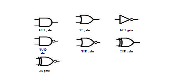
image.png
How to build a circuit utilizing a door unit?
The circuit built by the gate unit is called the gate circuit. According to a certain logic relationship, different gate units are connected to realize the logic function we need. This is the purpose of digital circuit design. Here are two examples of using a logic gate unit to build a half adder and a full adder gate circuit:
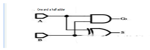
image.png
The figure above is a half-adder circuit constructed by an AND gate and an XOR gate, where A and B are the input signals of the half adder, S is the result output of the half adder, C is the carry input of the half adder.
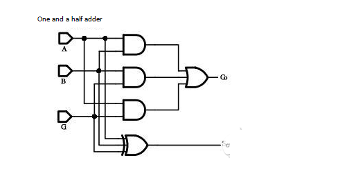
image.png
The above figure is a full adder circuit built by the logic gate unit. A and B are the input signals of the full adder, Ci is the carry input signal of the full adder, S is the full adder result output, and Co is the  carry output of the full adder.

Why can I implement the addition function? The following is a simple analysis of the principle of the addition function of the above two gate circuits. First, explain the difference between the half adder and the full adder: the half adder only adds the input signals A and B regardless of the carry; the full adder adds the carry Ci in addition to the A and B additions.

Among them, the half adders are added, and only when A and B are both 1, the addition will generate a carry, so Co=A&B. When both A and B are 0, the addition result S=0. Only one of A and B is 0 and the other is 1, the addition result S=1, so S=A^B.

The operation of the full adder is a bit more complicated. When one or three of the three inputs A, B, and Ci are 1, the addition result S=1, otherwise S=0, so S=A^B^Ci; When any two or three of the three inputs A, B, and Ci are 1, the addition will result in a carry of Co = 1, otherwise Co = 0, so Co = A & B | A & C | B & C.

If you want to know more, our website has product specifications for logic gate circuit, you can go to ALLICDATA ELECTRONICS LIMITED to get more information

2019年10月9日星期三

Pin diagrams of infrared receivers and amplifier circuits, where are the differences, how should they be distinguished?

The principle of the infrared receiving head is that the infrared monitoring diode monitors the infrared signal, and then sends the signal to the amplifier and the limiter. The limiter controls the pulse amplitude to a certain level regardless of the distance between the infrared transmitter and the receiver. The AC signal enters the bandpass filter, the bandpass filter can pass the load wave from 30khz to 60khz, enter the comparator through the demodulation circuit and the integration circuit, and the comparator outputs high and low levels to restore the signal waveform of the transmitter.

The infrared receiving head is an integrated receiving head composed of an infrared receiving tube and an amplifying circuit. The amplifying circuit is usually composed of an integrated block and a plurality of resistors and capacitors, and needs to be packaged in a metal shielding box, so that the circuit is complicated and the volume is small.

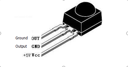
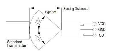
There are many types of infrared receivers, and the pin definitions are different. Generally, there are three pins, including power supply pins, grounding and signal output pins. The receiving head of the corresponding demodulation frequency should be selected according to the difference of the modulated carrier at the transmitting end.
image.png
Because the engineering process is to insert the board after spot welding, the project needs to understand the pins of the infrared receiver to make the pins correctly pair the board. So how do you identify the three pins of the infrared receiver?
image.png
There are generally two methods, the first one is the simplest, let the infrared receiver supplier provide the model specification, through the specification to distinguish the pins of the receiver. The other is to use the mechanical meter to measure the resistance of the two pins, find the one with the lowest resistance of the two pins. At this time, the watch stick should not move. The red watch stick is connected to Vcc, the watch stick is grounded, and the other pin is the signal pin(IR).

The three pins of the infrared receiver are GND, Vcc, and Out pins, which are ground, power, and signal outputs. Different types of infrared receivers have different pinouts.
image.png
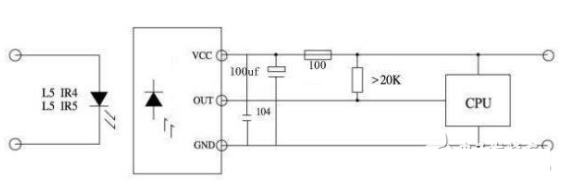
The gain of the internal amplifier of the infrared receiving head is very large, which is easy to cause interference. Therefore, the VCC (voltage) PIN pin and the GND (ground) pin of the receiving head must be added with a filter capacitor. The expert test test is generally performed on a 47uf ceramic capacitor ( Note: Adding a capacitor to a 100uf or 20UF capacitor will cause the receiver to receive a short distance.

Infrared integrated receiving head: The infrared receiving head is generally a receiving, amplifying and demodulating integrated head. After the infrared signal is demodulated by the receiving head, the difference between the data “0” and “1” is usually reflected in the length of the high and low level or During the signal cycle, when the MCU decodes, the output pin of the receiving head is usually connected to the external interrupt of the MCU, and the time of the external interrupt interval is judged by the timer to obtain the data. The point is to find the difference in waveform between the data "0" and "1". The output can be connected to CMOS and TTL circuits. This type of receiver is widely used in air conditioners, TVs, VCDs and other electrical appliances.
If you want to know more, our website has product specifications for the infrared receiver and the amplifier circuit, you can go to ALLICDATA ELECTRONICS LIMITED to get more information
2019年9月27日星期五

Connectors are a very important part of electronics

In today's era of so advanced technology, there are many electronic products that we use or touch in real life. Imagine what would happen if there were no connectors in electronic products. The circuits of electronic products should be permanently connected with continuous conductors. Together, for example, an electronic device is to be connected to a power source, and both ends of the connecting wire must be fixedly fastened to the electronic device and the power source by some method (welding).
As mentioned above, both the manufacture of the product and the use of the finished electronic product bring a lot of inconvenience. Taking the LED landscape light as an example, the distance from the power supply to the lamp holder is generally relatively large. If each line is connected from head to tail from the power supply to the lamp holder, it will bring unnecessary trouble to the construction and cause Wire wasted.

Some people may ask questions, directly open a gap from the fire line, connect the conductive parts of the wire together, and then wrap a few layers of insulating glue is not OK? It is not necessary to use a connector. Firstly, most of the insulating tapes are easy to age, and there are safety hazards. Secondly, the mechanical properties of the joints directly connected by wires are very poor. The wires are slightly vibrated and stretched, which is easy to cause an open circuit, and the interface is poorly contacted, which may cause heat generation, which may cause a fire.

Moreover, the outdoor environment is harsh, the requirements of waterproofing, salt-proof and anti-aging will be relatively high, and the insulating rubber will not meet the requirements. But if you use high-performance waterproof connectors in outdoor lighting, it not only simplifies the installation of the power grid, but also all the safety hazards will be reduced to a very low level.

The above example simply illustrates the benefits of the connector, which makes the design and production process more convenient, more flexible, safer, and lowers production and maintenance costs. The emergence of connectors improves the manufacturing process. The connector simplifies the assembly process of electronic products, and simplifies the mass production process. It is easy to repair. If an electronic component fails, the failed component can be quickly replaced when the connector is installed, and the upgrade is easy. Replacing components with connectors, replacing old design flexibility with new, more sophisticated components. Using connectors allows engineers to design and integrate new products, as well as when building components with components, Greater flexibility.

Especially for industrial connectors, sometimes it is more important to be flexible and safe in harsh environments where plugging and unplugging is required. At this time, a simple plug connector with a snap button would be a wise choice.
image.png 

How can I improve electromagnetic compatibility?

Various forms of electromagnetic interference are the main factors affecting the electromagnetic compatibility of electrical equipment. Electromagnetic interference can be divided into internal interference and external interference. Internal interference refers to mutual interference between various components inside an electronic device. For example, the working power supply generates interference caused by leakage of distributed capacitance and insulation resistance of the line, interference of component heating, impedance interference of signal through ground wire, power supply and transmission wire, magnetic field and electric field interference generated by high-power and high-voltage components. External interference refers to interference caused by factors other than electronic equipment or systems. For example: interference caused by space electromagnetic waves, interference generated by power supply network, strong magnetic field interference generated by external high-power equipment, interference caused by external high voltage through insulation leakage, and disturbance caused by internal electronic components due to unstable environmental temperature Wait. In order to ensure the normal operation of medical electronic equipment, the impact of interference must be weakened and prevented. There must be three factors in the electromagnetic compatibility problem between the systems: electromagnetic interference source, coupling path, and sensitive equipment. These three aspects are indispensable. Therefore, we can take corresponding measures from the above three aspects, such as eliminating or suppressing interference source, cut off the interference channel and weaken the sensitivity of the equipment to interference, etc., by adopting various anti-interference technical measures, the equipment instrument works stably and reliably, and effectively solves the electromagnetic compatibility problem. Common techniques for suppressing interference are:
image.png
Electromagnetic shielding
The shielding body is used to absorb energy (eddy current loss), reflected energy (electromagnetic wave reflection at the interface of the shielding body) and offset energy for electromagnetic waves from the outside or inside (electromagnetic induction generates a reverse electromagnetic field on the shielding layer to cancel part of the interference). The role of electromagnetic waves, to achieve the function of reducing interference. When the frequency of the interfering electromagnetic field is high, a conductive metal material is used as a shielding layer, and the eddy current generated in the shielding metal by the high-frequency interference electromagnetic field is used to form a canceling effect of the external electromagnetic wave. When the frequency of the interfering electromagnetic field is low, a high magnetic permeability material is used as a shielding layer to limit the magnetic lines of force inside the shielding body to prevent outward diffusion.

In recent years, plastic cases, plastic parts or panels have been widely used in medical electronic devices, so that external electromagnetic waves can easily penetrate the outer casing or the panel, which interferes with the normal operation of the instrument, and the electromagnetic waves generated by the instrument are also very easy to radiate. Go to the surrounding space and affect the normal operation of other electronic instruments. Such instruments can be treated by a plastic metallization process, such as sputter galvanizing, electroless copper plating, pasting metal foil, and coating of a conductive coating. After metallization, the fully insulated plastic surface has a metal. This reflects, absorbs, conducts, and attenuates the characteristics of electromagnetic waves, and acts to shield electromagnetic waves. The Chinese and foreign instruments and devices with display function, because the display screen uses ordinary glass, does not have the function of electromagnetic shielding, and the electromagnetic waves generated by the internal module work radiate outward through here to form interference. In order to improve the electromagnetic compatibility of the instrument, the original display glass can be changed into a screened glass to cut off the electromagnetic coupling path.

Electrostatic shielding
It is shielded by a metal container with good conductivity connected to the ground, so that the internal electric field is not transmitted, and the external electric field does not affect the inside.

Ground
Grounding is the main method to suppress noise and prevent interference, including power system grounding, equipment grounding, circuit signal grounding, shield grounding, etc. The main purpose of grounding is:
(1) Make all the unit circuits in the whole circuit system have a common reference zero potential to ensure stable operation of the circuit system.
(2) Prevent interference from external electromagnetic fields. By grounding the casing, a large amount of electric charge accumulated on the casing due to electrostatic induction is transmitted to the earth, and the high voltage formed by these charges is prevented from interfering with the device.
 (3) Ensure safe work. In order to prevent damage caused by lightning strikes and personal safety of the workers, the casing of the electronic device must be connected to the earth. In order to prevent electromagnetic interference between the medical electronic devices sharing the power supply through the power line, a three-phase five-wire and single-phase three-wire power supply mode should be adopted. The grounding network must be standardized in the hospital. All kinds of grounding should be self-contained and cannot share the same grounding pole. There should be an independent AC grounding grid in the medical building, and no multi-point grounding is allowed in each room. It is forbidden to use the heating pipe and the water pipe as the grounding wire. It is strictly forbidden to work without the grounding wire.

Filtering is an important measure to suppress and prevent interference. According to the signal and noise frequency distribution range, the filter of the corresponding frequency band is connected into the signal transmission channel, and the noise is filtered or as much as possible to achieve the purpose of improving the signal to noise ratio. The use of a filtering network is a powerful measure to suppress interference sources and eliminate interference coupling, or to enhance the anti-jamming capability of receiving devices. There are many types of filters, such as low-pass filters, high-pass filters, band-pass filters, band-stop filters, etc. Depending on the characteristics of the signal spectrum and the spectral characteristics of the interference, choosing the appropriate filter can eliminate unwanted coupling. For example, a high-frequency circuit can use a CLCπ-type filter composed of two capacitors and one inductor (high-frequency choke). Decoupling and sensing decoupling networks isolate the circuit from the power supply, eliminate coupling between the circuits, and prevent interfering signals from entering the circuit.
Balance circuit
Also known as a symmetrical circuit, it refers to two wires in a two-wire circuit and all circuits connected to the wires, and have the same impedance to ground or to other wires. The purpose is to make the interference signals detected by the two wires equal. The interference noise at this time is a common state signal, which can disappear on the load itself.

Floating
Also known as floating, floating, refers to the electronic signal instrumentation of the input signal amplifier public line is not connected to the chassis and does not connect to the ground, a measure to suppress interference. The goal is to block the path of the interference current.

Isolation
Isolation is a technical measure to destroy the interference path and cut off the noise coupling channel to achieve the purpose of suppressing interference. Commonly used circuit isolation methods are transformer isolation method and photoelectric coupling method.
If you want to know more, our website has product specifications for accessories, you can go to ALLICDATA ELECTRONICS LIMITED to get more information
2019年9月19日星期四

Introduction to monolithic and mixed digital-to-analog converters

This article briefly introduces Monolithic/Hybrid Digital to Analog Converters
DIGITAL TO ANALOG CONVERTERS,both of them have been designed for four inputs. But, if the number of inputs is more than four, the combination of output becomes more than 16. This makes the circuit more complex and the accuracy of the circuit reduces. Therefore, in critical and complex applications, a monolithic/hybrid D/A converter IC must be used. With the help of binary-weighted resistor, and R  and 2R resistor methods, 8-bit,10-bit, 12-bit, 14-bit, and 16-bit D/A converters can be designed with a current output, voltage output, or both current and voltage outputs.
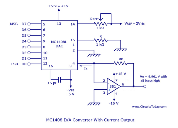
The most commonly used 8-bit D/A converter is MC 1408 which has a current output that can be converted to a voltage type using a current to voltage converter op-amp. The design along with the current to voltage converter is shown in the figure below.
image.png
MC 1408 Digital to Analog Converter
V0 = Vref/Rref *(RF)*{D7/2 + D6/4 + D5/8 + D4/16 + D3/32 + D2/64 + D1/128 + D0/256}
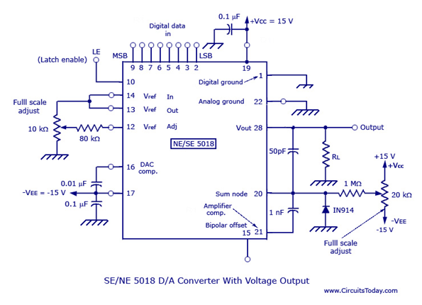
SE/NE 5018 is a typical 8-bit D/A converter with voltage output. The figure is shown below.
image.png
SE-NE 5018 Digital to Analog Converter
In the figure, the SE/NE 5018 circuit is configured for uni-polar output (0V to 10V). For 12 bits of resolution as well as current and voltage outputs, hybrid D/A converters such as DATEL DAC-H2 series is used.
For the correct selection of the D/A converter out of the lot, some important specifications of the converter must be known.
This article is from Allicdata Electronics Limited. Reprinted need to indicate the source.

2019年9月18日星期三

What is a gas sensor and what type of sensor?

1.The role of the gas sensor.
The device that can sense the change of gas sensing concentration is called gas sensor. Gas sensors are widely used in petroleum, mining, machinery, chemical and other light and heavy industries as well as ordinary families about gas poisoning and fire, detection, alarm and control of accidents such as explosion and air pollution. In industrial production and people's daily life, gas sensors are widely used to detect the leakage of combustible gases and toxic gases, in case of air pollution, explosion, fire, poisoning, etc. There are many kinds of gas sensors, and the most common ones are semiconductor gas sensors.

2.The characteristics of the gas sensor.
Semiconductor gas sensor is the core of semiconductor gas sensor. It is made of the characteristic that the semiconductor material SnO2can adsorb the gas to change its resistance. When the detected gas is adsorbed on its surface, the proportion of conductive electrons in the contact interface of the semiconductor crystallite particles will change, so that the resistance value of the gas sensor will be changed measuring the concentration of the gas changes, so the gas concentration can be converted into the change of the Telecom number. This reaction is reversible and therefore reusable.
In order to speed up the reaction and achieve high sensitivity, it is usually necessary to heat the gas sensor with electric current through the heating wire. The heating temperature varies with the material used by the gas sensor. When the gas sensor starts heating in the clean air, the resistance drops sharply, and the stable value is reached after a few minutes, which is called the passive period stabilization time. When the resistance of the gas sensor is in the stable value, it will change with the adsorption of the detected gas. The variation of resistance depends on the type of semiconductor. The resistance of P-type semiconductor gas sensor increased, and the resistance of N-type semiconductor gas sensor decreased. After the gas sensor is heated, the resistance in the normal air is the static resistance Ro, and the resistance value of the gas sensor is Rx, the ratio of Ro to Rx is called the sensitivity of the gas sensor. When the gas sensor is in contact with the detected gas, the time of its resistance changing from Ro to Rx is called the response time; when the gas is removed, the time of recovery from Rx to Ro is called recovery time.

3.Choose a gas sensor in use.
(1)The sensitivity of the measured gas is high, and the variation of resistance per unit gas concentration is large.
(2) Good selectivity for single or multiple measured gases is less dependent on the temperature of the environment.
(4) Good moisture resistance.
(5) Long life.
To understand their aging mechanisms, they can predict their lifespan.

4.Detect the gas sensor.
 Add voltage to the gas sensor, when the gas sensor is connected to the circuit, the voltmeter pointer should be deflected in the negative direction and go back to zero after a few seconds, and then gradually rise to a stable value, indicating that the gas sensor has reached the preheating time. The ammeter should be indicated within 150mA, with some gas (such as alcohol, liquefied gas and so on) aiming at the gas sensitivity. Probe, use a multimeter to measure the voltage at both ends of Uo.
The gas should change, no change is bad. (the greater the amplitude of the voltmeter is, the better the performance of the gas sensor.)

If you want to know more, our website has product specifications for gas sensors, you can go to ALLICDATA ELECTRONICS LIMITED to get more information
Gas Sensors  CCS811B-JOPD500
 LOW POWER DIGITAL SENSOR FOR INDAir Quality Sensor I²C

CCS811B-JOPD500 Allicdata Electronics

2019年9月17日星期二

New amplifier with audio - IC and multi-chip modules

Infineon is combining its existing line of amplifiers with audio applications - IC and multi-chip modules. Four new Merus brand IC amplifiers have been proposed.

With its new "Merus" brand for audio amplifier ICs, Infineon wants to highlight the advantages of its amplifier ICs:
1. When the sound is generated in the speaker, the heat is not distributed;
2. Can't see, but can hear it;
3. Small and light;
4. Be flexible and configurable, but not just delicate and difficult to use.

The Merus amplifier is based on a new technology: multi-stage switching technology for Class D audio amplifiers, comparable to multi-level converter technology. Not only does it provide high efficiency, but it also has a positive impact on other audio amplifiers such as sound quality, size, output power, electromagnetic emissions and component costs.

Under the new Merus brand, Infineon bundles its amplifier ICs for audio applications.
Infineon is modulating the new Class D audio amplifier to control the power level of the analog five-speed converter. These multistage Class D amplifiers use additional power MOSFETs (integrated in the IC) and capacitors compared to conventional amplifiers.
This technique makes it possible to output an audio signal with a higher granularity, ie with a higher switching frequency and a scalable output signal level. Another advantage of multi-stage Class D amplifiers: they allow for smaller designs and sleep modes with virtually no measurable switching losses.

Four new Merus amplifiers
Based on the new modulation technology, Infineon introduces one of four integrated multi-stage class D audio amplifiers: the MA12040 and MA12070 with analog audio inputs, MA12040P and MA12070P with digital inputs (I 2 S). They are satisfied with power consumption in the 250 mW range and have no output filter. Therefore, they are particularly suitable for portable battery powered devices and for applications with limited installation space - if there is no space for the heat sink and the output filter is present.

The new Merus Class D amplifiers from the Infineon MA12040 / P and MA12070 / P support up to four channels.
Traditional Class D amplifiers operate only at higher volume levels and are more efficient. A realistic and typical audio playback that requires an average of about 1 watt of output power for itself is much more power than the IC of the first generation Merus multi-stage class d audio amplifier now presented.
The new audio amplifier IC supports up to four channels in the mode PBTL (parallel bridge load), BTL (bridged load) or SE (single-ended) can be configured. In PBTL mode, a single monolithic IC can deliver up to 160 W of peak power - maximum. 16 A load current. Alternatively, a four-channel IC can also be used in a 2.1 system, for example, two to drive a 20 watt range speaker (SE mode) and a 40 W woofer (BTL mode).
The new Merus Class D amplifiers, the MA12040/P and MA12070/P, have an integrated digital power supply with low distortion (THD + N = 0.003%) and low EMI emissions. They are protected by a variety of built-in functions: undervoltage shutdown (UVLO), short/overcurrent and DC protection, and warning and error messages when overheating. Infineon offers an integrated Merus Class Daudio amplifier IC in a thermally optimized 64-pin QFN package with EPAD (exposed thermal pad).

What is the development status and trend of led display?

  Over the past few years, with the further release of the market, the entire LED display industry has regained its vitality, and market com...